ILA7056B
ILA7056B is 5 W Mono BTL Audio Amplifier manufactured by IK Semiconductor.
FEATURES
- -
- -
- -
- -
- - DC volume control Few external ponents Mute mode Thermal protection Short-circuit proof No switch-on and switch-off clicks Good overall stability Low power consumption Low HF radiation ESD protected on all pins
ORDERING INFORMATION Plastic SIL-9MPF (SOT110-1)
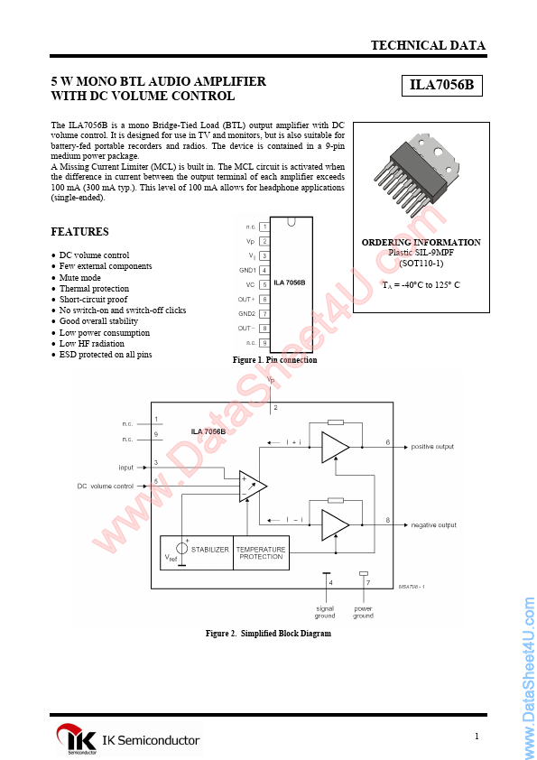
Figure 1. Pin connection w w w t a .D
S a e h
U 4 t e
.c m o
TA = -40°C to 125° C
Figure 2. Simplified Block Diagram
..
MAXIMUM RATINGS SYMBOL VP V3, 5 IORM IOSM Ptot Tamb Tstg Tvj Tsc PARAMETER supply voltage input voltage pins 3 and 5 repetitive peak output current non-repetitive peak output current total power dissipation operating ambient temperature storage temperature virtual junction temperature short-circuit time CONDITIONS MIN -40 -55 MAX 18 5 1.25 1.5 9 +85 +150 +150 1 UNIT V V A A W ° C ° C ° C h
Tcase < 60ºC
ELECTRICAL CHARACTERISTICS VP = 12 V; VDC = 1.4 V; f = 1 k Hz; RL = 16 Ω; Tamb = 25 °C; unless otherwise specified (see Fig.13). SYMBOL PARAMETER Supply VP positive supply voltage Iq(tot) total quiescent current Maximum gain (V5 ≥ 1.4 V) PO output power THD total harmonic distortion Gv(max) maximum total voltage gain VI input signal handling (RMS value) Vno noise output voltage (RMS value) B bandwidth SVRR supply voltage ripple rejection DC output offset voltage ⏐∆VO⏐ ZI input impedance (pin 3) Mute position VO output voltage in mute position DC volume control; note 5 Φ gain control I5 control current
Notes
CONDITIONS note 1; RL = ∞ THD = 10%; RL = 16 Ω THD = 10%; RL = 8 Ω PO = 0.5 W Gv(max) = 0 d B; THD <1% note 2; f = 500 k Hz at
- 1d B note 3 ⏐V8
- V6⏐ note 4; V5 = 0.4 V ±30 m V VI = 1.0 V V5 = 0 V
MIN 4.5
- 3
- - 39.5 1.0
- - 34
- 15
- - 9.2
MAX 18 13
- - 1 41.5
- -
- - 200 25 40
UNIT V m A W W % d B V µV k Hz d B m V k Hz µV
3.5 5 0.3 40.5
- 210 0.02 to 300 38 0 20 30
68 20
73.5 25
- 30 d B µA
1. With a load connected to the outputs the quiescent current will increase, the maximum value of this increase being equal to the DC output offset...