IN7440
TECHNICAL DATA
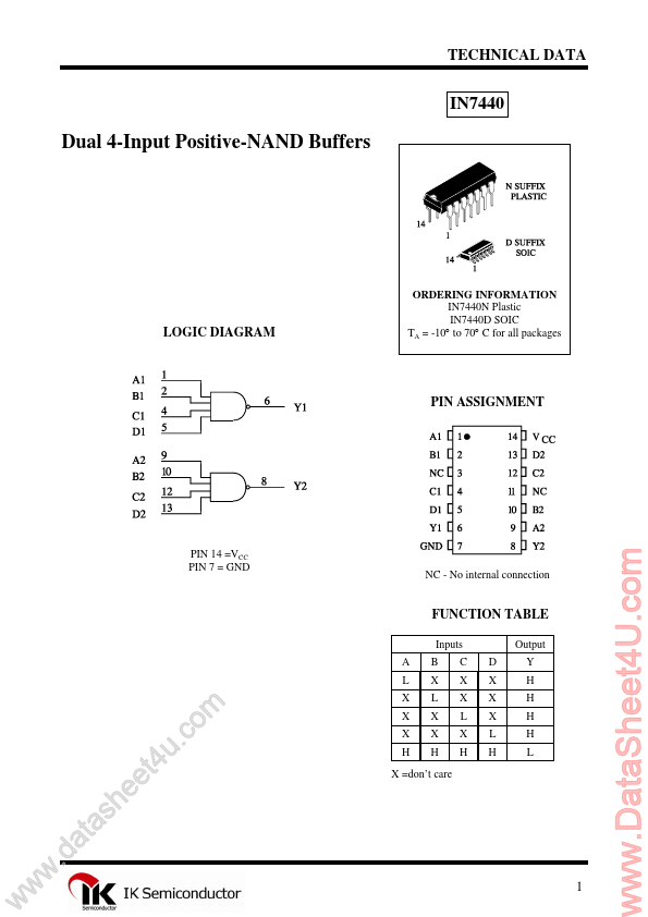
Dual 4-Input Positive-NAND Buffers
LOGIC DIAGRAM
ORDERING INFORMATION IN7440N Plastic IN7440D SOIC TA = -10° to 70° C for all packages
PIN ASSIGNMENT
PIN 14 =VCC PIN 7 = GND
- No internal connection
FUNCTION TABLE
Inputs A L X X X H B X L X X H C X X L X H D X X X L H Output Y H H H H L w w w
.d h s a t a ee
. u t4 m o c
X =don’t care
..
MAXIMUM RATINGS-
Symbol VCC VIN IOL Tstg
- Parameter Supply Voltage Input Voltage Low Level Output Current Storage Temperature Range
Value 7.0 5.5 48 -65 to +150
Unit V V m A °C
Maximum Ratings are those values beyond which damage to the device may occur. Functional operation should be restricted to the Remended Operating Conditions.
REMENDED OPERATING CONDITIONS
Symbol VCC VIH VIL IOH IOL TA Supply Voltage High Level Input Voltage Low Level Input Voltage High Level Output Current Low Level Output Current Ambient Temperature Range -10 Parameter Min 4.75 2.0 0.8 -1.2 48 +70 Max 5.25 Unit V V V...