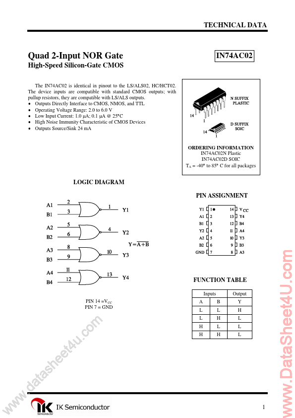
IN74AC02
TECHNICAL DATA
Quad 2-Input NOR Gate
High-Speed Silicon-Gate CMOS
The IN74AC02 is identical in pinout to the LS/ALS02, HC/HCT02. The device inputs are patible with standard CMOS outputs; with pullup resistors, they are patible with LS/ALS outputs.
- Outputs Directly Interface to CMOS, NMOS, and TTL
- Operating Voltage Range: 2.0 to 6.0 V
- Low Input Current: 1.0 µA; 0.1 µA @ 25°C
- High Noise Immunity Characteristic of CMOS Devices
- Outputs Source/Sink 24 m A
ORDERING INFORMATION IN74AC02N Plastic IN74AC02D SOIC TA = -40° to 85° C for all packages
LOGIC DIAGRAM PIN ASSIGNMENT
FUNCTION TABLE
Inputs PIN 14 =VCC PIN 7 = GND A L L H H B L H L H Output Y H L L L w w w
.d e e h s a t a
. u t4 m o c
..
MAXIMUM RATINGS-
Symbol VCC VIN VOUT IIN IOUT ICC PD Tstg TL
- Parameter DC Supply Voltage (Referenced to GND) DC Input Voltage (Referenced to GND) DC Output Voltage (Referenced to GND) DC Input Current, per Pin DC Output Sink/Source Current, per Pin DC...