IN74HC02A
Overview
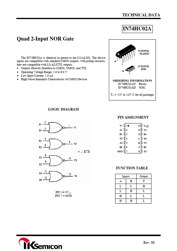
Quad 2-Input NOR Gate TECHNICAL DATA IN74HC02A The IN74HC02A is identical in pinout to the LS/ALS02. The device inputs are compatible with standard CMOS outputs; with pullup resistors, they are comp...
| Part | IN74HC02A |
|---|---|
| Description | Quad 2-Input NOR Gate |
| Manufacturer | IK Semiconductor |
| Size | 182.75 KB |
Quad 2-Input NOR Gate TECHNICAL DATA IN74HC02A The IN74HC02A is identical in pinout to the LS/ALS02. The device inputs are compatible with standard CMOS outputs; with pullup resistors, they are comp...