IN74HC21A
IN74HC21A is Dual 4-Input Positive-AND Gate manufactured by IK Semiconductor.
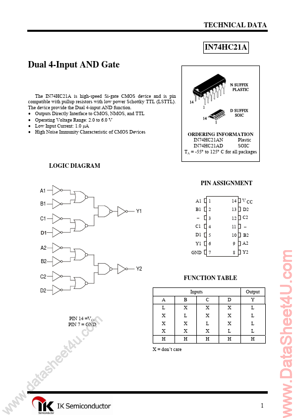
TECHNICAL DATA
Dual 4-Input AND Gate
The IN74HC21A is high-speed Si-gate CMOS device and is pin patible with pullup resistors with low power Schottky TTL (LSTTL). The device provide the Dual 4-input AND function.
- Outputs Directly Interface to CMOS, NMOS, and TTL
- Operating Voltage Range: 2.0 to 6.0 V
- Low Input Current: 1.0 µA
- High Noise Immunity Characteristic of CMOS Devices
ORDERING INFORMATION IN74HC21AN Plastic IN74HC21AD SOIC TA = -55° to 125° C for all packages
LOGIC DIAGRAM PIN ASSIGNMENT
A1 B1 Y1 C1
C1 D1 A1 B1
1 2 3 4 5 6 7
14 13 12 11 10 9 8
V CC
D2 C2
B2 A2 Y2
B2 Y2 C2 D2
FUNCTION TABLE
Inputs A L
PIN 14 =VCC PIN 7 = GND
Output С X X L X H D X X X L H Y L L L L H
B X L X X H w w w a t a d . e h s et
4u m o .c
X X X H X = don’t care
..
A2
Y1
MAXIMUM RATINGS-
Symbol VCC VIN VOUT IIN IOUT ICC PD Tstg TL Parameter DC Supply Voltage (Referenced to GND) DC Input Voltage (Referenced to GND) DC Output Voltage (Referenced to GND) DC Input Current, per Pin DC Output Current, per Pin DC Supply Current, VCC and GND Pins Power Dissipation in Still Air, Plastic DIP-
- SOIC Package-
- Storage Temperature Lead Temperature, 1 mm from Case for 10 Seconds (Plastic DIP or SOIC Package) Value -0.5 to +7.0 -1.5 to VCC +1.5 -0.5 to VCC +0.5 ±20 ±25 ±50 750 500 -65 to +150 260 Unit V V V m A m A m A m W °C °C
- Maximum Ratings are those values beyond which damage to the device may occur. Functional operation should be restricted to the Remended Operating Conditions.
- - Derating
- Plastic DIP:
- 10 m W/°C from 65° to 125°C SOIC Package: :
- 7 m W/°C from 65° to 125°C
REMENDED OPERATING CONDITIONS
Symbol VCC VIN, VOUT TA tr, tf Parameter DC Supply Voltage (Referenced to GND) DC Input Voltage, Output Voltage (Referenced to GND) Operating Temperature, All Package Types Input Rise and Fall Time (Figure 1) VCC =2.0 V VCC =4.5 V VCC =6.0 V Min 2.0 0 -55 0 0 0 Max 6.0 VCC +125 1000 500 400 Unit V V °C...