IN74HC251A
feature allows the IN74HC251A to be used in bus-oriented systems.
- Outputs Directly Interface to CMOS, NMOS, and TTL
- Operating Voltage Range: 2.0 to 6.0 V
- Low Input Current: 1.0 µA
- High Noise Immunity Characteristic of CMOS Devices
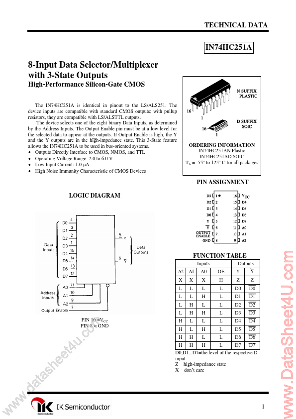
ORDERING INFORMATION IN74HC251AN Plastic IN74HC251AD SOIC TA = -55° to 125° C for all packages
PIN ASSIGNMENT LOGIC DIAGRAM
FUNCTION TABLE
Inputs A2 X L L L L PIN 16 =VCC PIN 8 = GND A1 X L L H H L L H A0 X L H L H L H L OE H L L L L L L L Outputs Y Z D0 D1 D2 D3 D4 D5 D6 Y Z D0 D1 D2 D3 D4 D5 D6 w w w
.d e e h s a t a
. u t4 m o c
H H H L D7 D7 D0,D1...D7=the level of the respective D input Z = high-impedance state X = don’t care
..
MAXIMUM RATINGS-
Symbol VCC VIN VOUT IIN IOUT ICC PD Tstg TL
- Parameter DC Supply Voltage (Referenced to GND) DC Input Voltage (Referenced to GND) DC Output Voltage (Referenced to GND) DC Input Current, per Pin DC Output Current, per Pin DC Supply Current, VCC and GND Pins Power...