IN74HC273A
TECHNICAL DATA
Octal D Flip-Flop with mon Clock and Reset
High-Performance Silicon-Gate CMOS
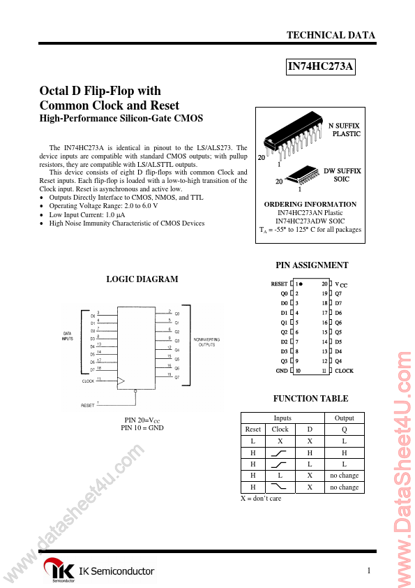
The IN74HC273A is identical in pinout to the LS/ALS273. The device inputs are patible with standard CMOS outputs; with pullup resistors, they are patible with LS/ALSTTL outputs. This device consists of eight D flip-flops with mon Clock and Reset inputs. Each flip-flop is loaded with a low-to-high transition of the Clock input. Reset is asynchronous and active low.
- Outputs Directly Interface to CMOS, NMOS, and TTL
- Operating Voltage Range: 2.0 to 6.0 V
- Low Input Current: 1.0 µA
- High Noise Immunity Characteristic of CMOS Devices
ORDERING INFORMATION IN74HC273AN Plastic IN74HC273ADW SOIC TA = -55° to 125° C for all packages
PIN ASSIGNMENT LOGIC DIAGRAM
FUNCTION TABLE
PIN 20=VCC PIN 10 = GND Inputs Reset L H H H H X = don’t care L Clock X D X H L X X Output Q L H L no change no change w w w
.d h s a t a ee
. u t4 m o c
..
MAXIMUM RATINGS-
Symbol VCC...