IN74LS04
IN74LS04 is Hex Inverter manufactured by IK Semiconductor.
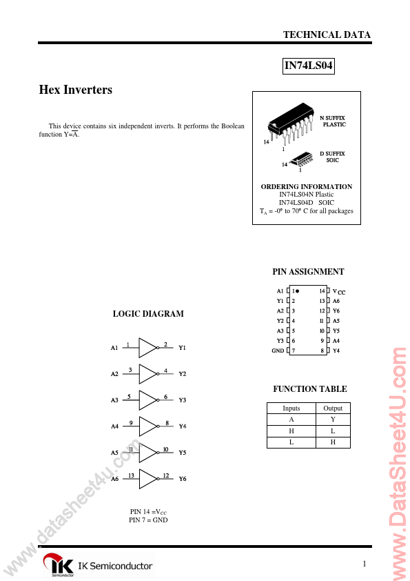
TECHNICAL DATA
Hex Inverters
This device contains six independent inverts. It performs the Boolean function Y=A.
ORDERING INFORMATION IN74LS04N Plastic IN74LS04D SOIC TA = -0° to 70° C for all packages
PIN ASSIGNMENT
LOGIC DIAGRAM
FUNCTION TABLE
Inputs A H L Output Y L H w w w
.d e e h s a t a
. u t4 m o c
PIN 14 =VCC PIN 7 = GND
..
MAXIMUM RATINGS-
Symbol VCC VIN VOUT Tstg
- Parameter Supply Voltage Input Voltage Output Voltage Storage Temperature Range
Value 7.0 7.0 7.0 -65 to +150
Unit V V V °C
Maximum Ratings are those values beyond which damage to the device may occur. Functional operation should be restricted to the Remended Operating Conditions.
REMENDED OPERATING CONDITIONS
Symbol VCC IOH IOL TA Supply Voltage High Level Output Current Low Level Output Current Ambient Temperature Range 0 Parameter Min 4.75 Max 5.25 -400 8.0 +70 Unit V V V °C
DC ELECTRICAL CHARACTERISTICS over full operating conditions
Guaranteed Limit Symbol VIH VIL VIK VOH VOL II IIH IIL IOS ICC Parameter High Level Input Voltage Low Level Input Voltage Input Clamp Voltage High Level Output Current Low Level Output Voltage Input Current at maximum input voltage High Level Input Current Low Level Input Current Short-circuit output current Supply Current VCC = min, II = -18 m A VCC = min, VIL =max IOH = max VCC = min, VIH =min, IOL = 8 m A VCC = max, VI = -7V VCC = max, VIN = 2.7 V VCC = max, VIN = 0.4 V VCC = max (Note) VCC = max Total with outputs high Total with outputs low -20 0.1 20 -0.4 -100 2.4 6.6 m A µA m A m A m A 0.5 V 2.7 Test Conditions Min 2 0.8 -1.5 Max Unit V V V V
Note: Not more than one output should be shorted at a time, and duration should not exceed one second.
AC ELECTRICAL CHARACTERISTICS (VCC = 5.0 V, CL = 15 p F, TA=25 °C, RL = 2 kΩ, tr =15 ns, tf = 6.0 ns) Symbol t PLH t PHL Parameter Propagation Delay Time Propagation Delay Time Min Max 15 15 Unit ns ns
Figure 1. Switching Waveforms
NOTE A. CL includes probe and...