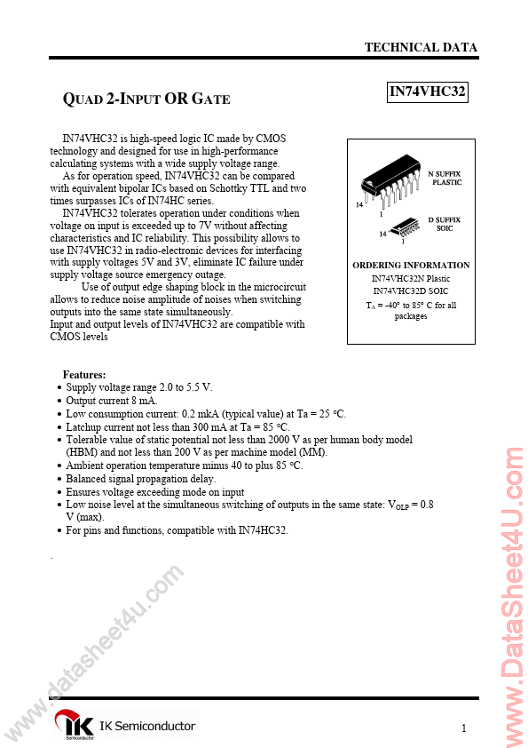
IN74VHC32
Overview
- Supply voltage range 2.0 to 5.5 V.
- Output current 8 mA.
- Low consumption current: 0.2 mkA (typical value) at Та = 25 °С.
- Latchup current not less than 300 mA at Та = 85 °С.
- Tolerable value of static potential not less than 2000 V as per human body model (HBM) and not less than 200 V as per machine model (ММ).
- Ambient operation temperature minus 40 to plus 85 °С.
- Balanced signal propagation delay.
- Ensures voltage exceeding mode on input
- Low noise level at the simultaneous switching of outputs in the same state: VOLP = 0.8 V (max).
- For pins and functions, compatible with IN74НС32.