IN74VHC74
Overview
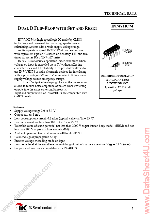
TECHNICAL DATA DUAL D FLIP-FLOP WITH SET AND RESET IN74VHC74 is high-speed logic IC made by CMOS technology and designed for use in high-performance calculating systems with a wide supply voltage ran...
| Part | IN74VHC74 |
|---|---|
| Description | Quad 2-Input OR Gate |
| Manufacturer | IK Semiconductor |
| Size | 280.34 KB |
TECHNICAL DATA DUAL D FLIP-FLOP WITH SET AND RESET IN74VHC74 is high-speed logic IC made by CMOS technology and designed for use in high-performance calculating systems with a wide supply voltage ran...