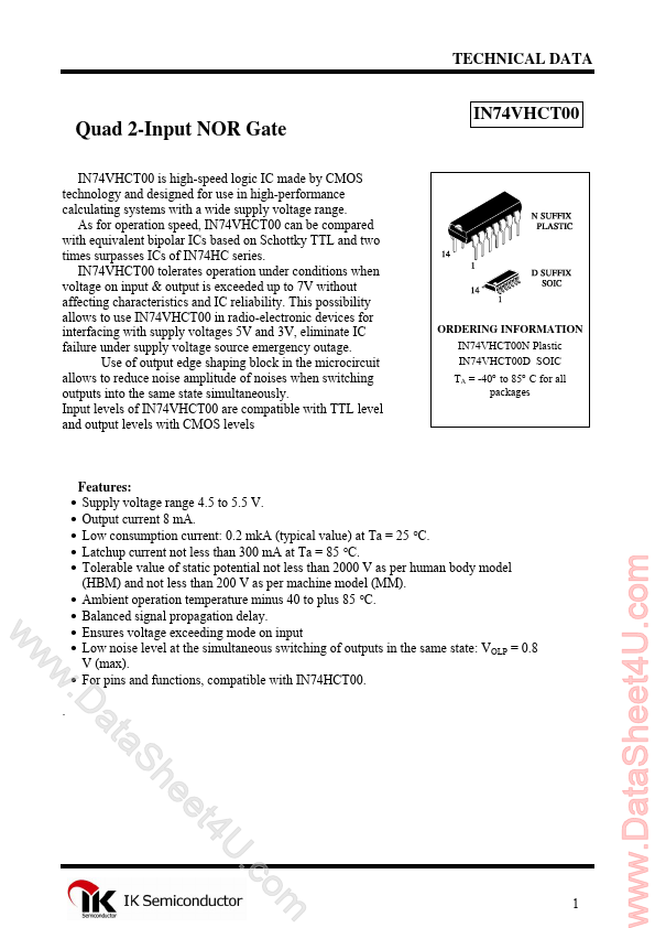
IN74VHCT00
Features
:
- Supply voltage range 4.5 to 5.5 V.
- Output current 8 m A.
- Low consumption current: 0.2 mk A (typical value) at Та = 25 °С.
- Latchup current not less than 300 m A at Та = 85 °С.
- Tolerable value of static potential not less than 2000 V as per human body model (HBM) and not less than 200 V as per machine model (ММ).
- Ambient operation temperature minus 40 to plus 85 °С.
- Balanced signal propagation delay.
- Ensures voltage exceeding mode on input
- Low noise level at the simultaneous switching of outputs in the same state: VOLP = 0.8 V (max).
- For pins and functions, patible with IN74HCT00.
IN74VHCT00 truth table
Input A L L H B L H L Output Y= A
- B H H H L
H H Note
- H
- high voltage level; L
- low voltage level;
Pinout
A1 01
B1 02
Y1 03
A2 04
B2 05
Y2 06
GND 07
Vcc B4 A4
11 Y4
B3 A3 Y3
Pins description in IN74VHCT00 Pin No. Symbol Description
01 А1 Input 02 В1 Input 03 Output Y1 04 А2 Input 05 В2 Input 06 Output Y2 07 GND mon...