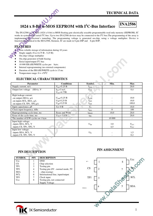
INA2586
Overview
- Non-volatile storage of information during 10 years Single supply (Ucc=4,75 B - 5,25 B) On-chip voltage multiplier On-chip generator of bulk biasing Serial input/output I2C-bus 10 000 ERASE/WRITE cycles per byte; Internal reprogramming (no external components) Duration of the ERASE/WRITE cycle is 15 ms Temperature range: 0 ÷ +700C m o .c