IW4502B
IW4502B is Hex Inverter/Buffer manufactured by IK Semiconductor.
TECHNICAL DATA
Strobed Hex Inverter/Buffer
High-Voltage Silicon-Gate CMOS
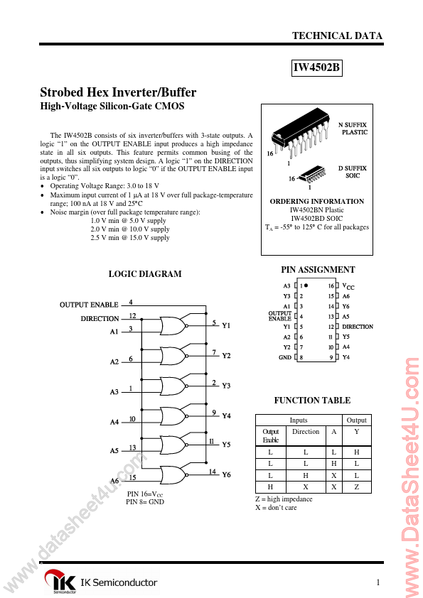
The IW4502B consists of six inverter/buffers with 3-state outputs. A logic “1” on the OUTPUT ENABLE input produces a high impedance state in all six outputs. This feature permits mon busing of the outputs, thus simplifying system design. A logic “1” on the DIRECTION input switches all six outputs to logic “0” if the OUTPUT ENABLE input is a logic “0”.
- Operating Voltage Range: 3.0 to 18 V
- Maximum input current of 1 µA at 18 V over full package-temperature range; 100 n A at 18 V and 25°C
- Noise margin (over full package temperature range): 1.0 V min @ 5.0 V supply 2.0 V min @ 10.0 V supply 2.5 V min @ 15.0 V supply
ORDERING INFORMATION IW4502BN Plastic IW4502BD SOIC TA = -55° to 125° C for all packages
LOGIC DIAGRAM
PIN ASSIGNMENT
FUNCTION TABLE
Inputs Output Enable Direction L L H X A L H X X Output Y H L L Z w w w
.d e e h s a t a
. u t4 m o c
PIN 16=VCC PIN 8= GND
Z = high impedance X = don’t care
..
MAXIMUM RATINGS-
Symbol VCC VIN VOUT IIN PD PD Tstg TL
- Parameter DC Supply Voltage (Referenced to GND) DC Input Voltage (Referenced to GND) DC Output Voltage (Referenced to GND) DC Input Current, per Pin Power Dissipation in Still Air, Plastic DIP+ SOIC Package+ Power Dissipation per Output Transistor Storage Temperature Lead Temperature, 1 mm from Case for 10 Seconds (Plastic DIP or SOIC Package)
Value -0.5 to +20 -0.5 to VCC +0.5 -0.5 to VCC +0.5 ±10 750 500 100 -65 to +150 260
Unit V V V m A m W m W °C °C
Maximum Ratings are those values beyond which damage to the device may occur. Functional operation should be restricted to the Remended Operating Conditions. +Derating
- Plastic DIP:
- 10 m W/°C from 65° to 125°C SOIC Package: :
- 7 m W/°C from 65° to 125°C
REMENDED OPERATING CONDITIONS
Symbol VCC VIN, VOUT TA Parameter DC Supply Voltage (Referenced to GND) DC Input Voltage, Output Voltage (Referenced to GND)...