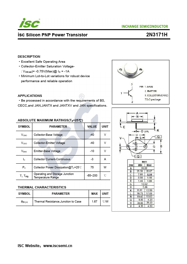
The following content is an automatically extracted verbatim text
from the original manufacturer datasheet and is provided for reference purposes only.
View original datasheet text
isc Silicon PNP Power Transistor
DESCRIPTION ·Excellent Safe Operating Area ·Collector-Emitter Saturation Voltage-
: VCE(sat)= -0.75V(Max)@ IC = -1A ·Minimum Lot-to-Lot variations for robust device
performance and reliable operation
APPLICATIONS ·Be processed in accordance with the requirements of BS, CECC,and JAN,JANTX and JANTXV and JAN specifications.
ABSOLUTE MAXIMUM RATINGS(Ta=25℃)
SYMBOL
PARAMETER
VALUE
UNIT
VCBO
Collector-Base Voltage
-40
V
VCEO Collector-Emitter Voltage
-40
V
VEBO
Emitter-Base Voltage
-10
V
IC
Collector Current-Continuous
-3
A
PC
Collector Power Dissipation@TC=25℃
75
W
TJ, Tstg
Operating and Storage Junction Temperature Range
-65~200 ℃
THERMAL CHARACTERISTICS
SYMBOL
PARAMETER
Rth j-c Thermal Resistance,Junction to Case
MAX UNIT 1.