Inchange Semiconductor 2SC1185
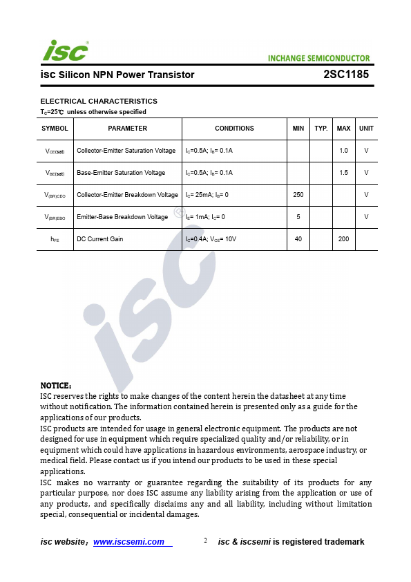
The information contained herein is presented only as a guide for the applications of our products. The products are not designed for use in equipment which require specialized quality and/or reliability, or in equipment which could have applications in hazardous environments, aerospace industry, or medical field.| Part No. | 2SC1185 |
|---|---|
| Datasheet | 2SC1185 Download |
| Manufacturer |  Inchange Semiconductor |
| Description | NPN Transistor |
| Buy | Stock & Price |
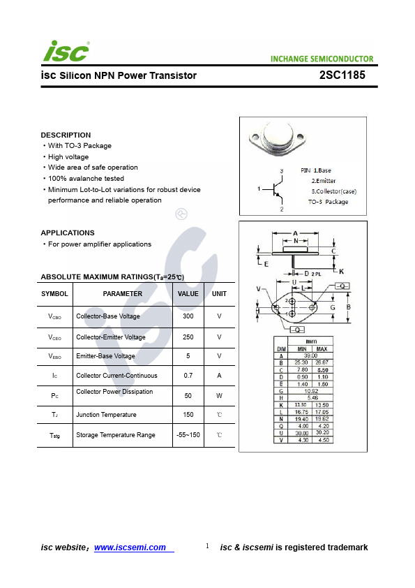
DESCRIPTION
●With TO-3 Package●High voltage
●Wide area of safe operation
●100% avalanche tested
●Minimum Lot-to-Lot variations for robust device performance and reliable operation
APPLICATIONS
●For power amplifier applicationsABSOLUTE MAXIMUM RATINGS
(Ta=25℃) SYMBOL PARAMETER VALUE UNIT VCBO Collector-Base Voltage VCEO VEBO IC PC TJ Collector-Emitter Voltage Emitter-Base Voltage Collector Current-Continuous Collector Power Dissipation Junction Temperature Tstg Storage Temperature Range 300 V 250 V 5 V 0.7 A 50 W 150 ℃ -55~150 ℃ isc website: 1 isc & iscsemi is registered trademark isc Silicon NPN Power Transistor INCHANGE Semiconductor 2SC1185ELECTRICAL CHARACTERISTICS
TC=25℃ unless otherwise specified SYMBOL PARAMETER CONDITIONS VCE(sat) Collector-Emitter Saturation Voltage IC=0.5A; IB= 0.1A VBE(sat) Base-Emitter Saturation Voltage IC=0.5A; IB= 0.1A V(BR)CEO Collector-Emitter Breakdown Voltage IC= 25mA; IB= 0 V(BR)EBO Emitter-Base Breakdown Voltage IE= 1mA; IC= 0 hFE DC Current Gain IC=0.4A; VCE= 10V MIN TYP.