2SC9014
Overview
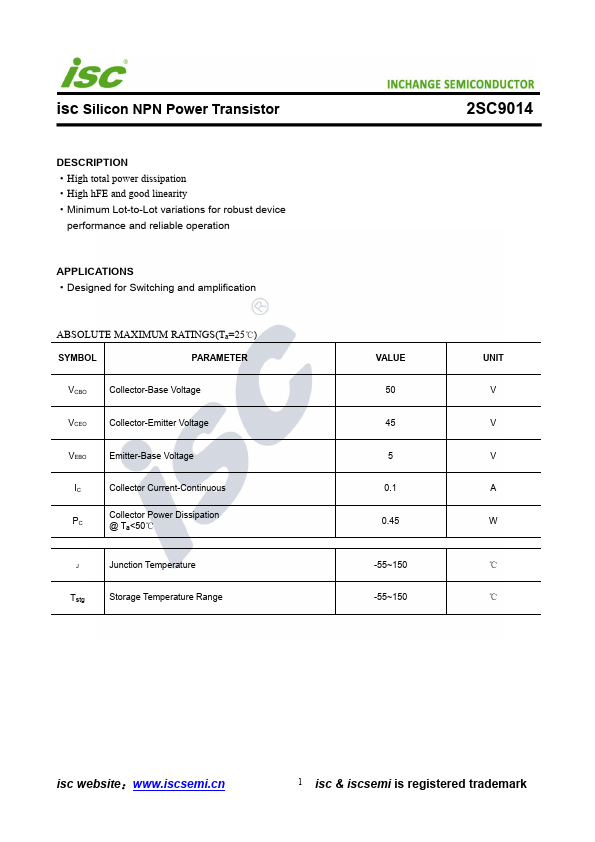
High total power dissipation High hFE and good linearity Minimum Lot-to-Lot variations for robust device performance and reliable operation.
| Part | 2SC9014 |
|---|---|
| Description | NPN Transistor |
| Category | Transistor |
| Manufacturer | Inchange Semiconductor |
| Size | 218.55 KB |
High total power dissipation High hFE and good linearity Minimum Lot-to-Lot variations for robust device performance and reliable operation.
| Part Number | Manufacturer | Description |
|---|---|---|
| 2SC9014 | USHA | Transistors |
| 2SC9016 | USHA | Transistors |
| 2SC9012 | Promax Johnton | PNP Transistor |
| C9015 | KEC | 2SC9015 |
| C9011 | USHA | 2SC9011 |