3DD523
DESCRIPTION
- Excellent safe operating area
- Low Collector-Emitter Saturation Voltage
- Minimum Lot-to-Lot variations for robust device performance and reliable operation
APPLICATIONS
- Designed for general purpose switching and amplifier applications
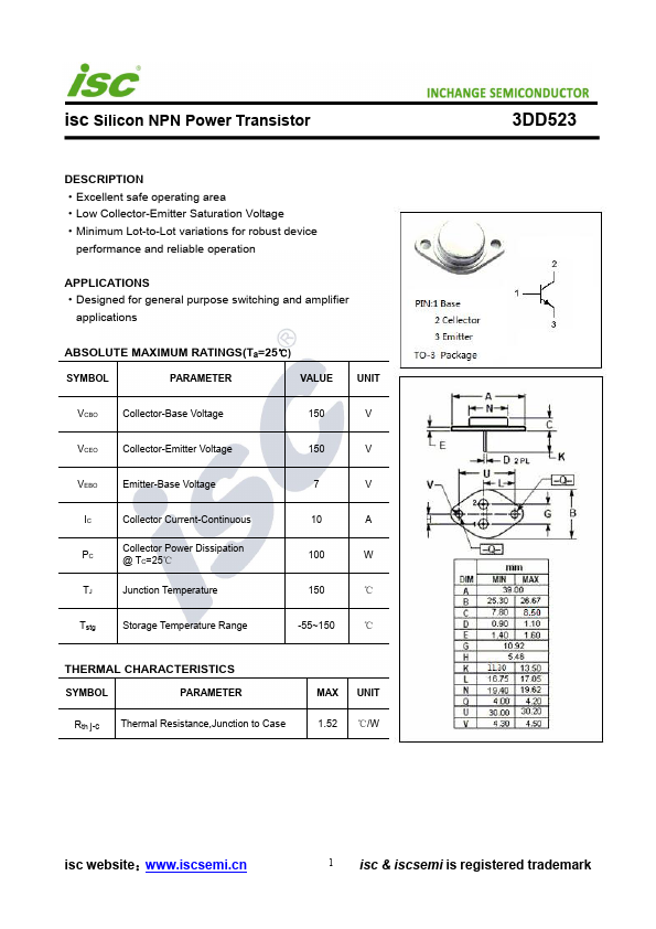
ABSOLUTE MAXIMUM RATINGS(Ta=25℃)
SYMBOL
PARAMETER
VALUE
UNIT
VCBO
Collector-Base Voltage
VCEO
Collector-Emitter Voltage
VEBO
Emitter-Base Voltage
Collector Current-Continuous
Collector Power Dissipation @ TC=25℃
Junction Temperature
℃
Tstg
Storage Temperature Range
-55~150
℃
THERMAL CHARACTERISTICS
SYMBOL
PARAMETER
Rth j-c Thermal Resistance,Junction to Case
MAX UNIT 1.52 ℃/W
3DD523 isc website:.iscsemi.cn
1 isc & iscsemi is registered trademark isc Silicon NPN Power Transistor
ELECTRICAL CHARACTERISTICS...