Inchange Semiconductor 7915
Three Terminal Negative Voltage Regulator
| Part No. | 7915 |
|---|---|
| Datasheet | 7915 Download |
| Manufacturer |  Inchange Semiconductor |
| Description | Three Terminal Negative Voltage Regulator |
| Buy | Stock & Price |
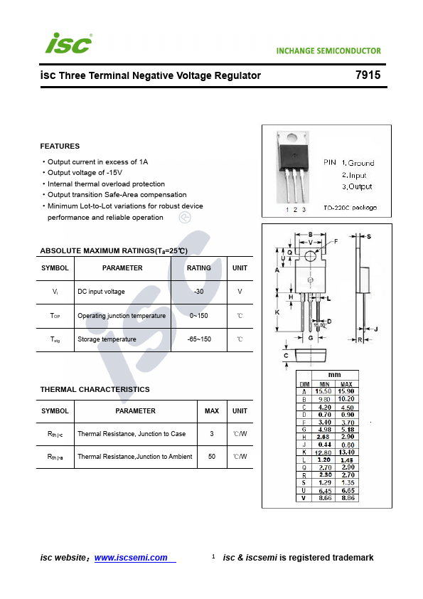
FEATURES
●Output current in excess of 1A●Output voltage of -15V
●Internal thermal overload protection
●Output transition Safe-Area compensation
●Minimum Lot-to-Lot variations for robust device performance and reliable operation
ABSOLUTE MAXIMUM RATINGS
(Ta=25℃) SYMBOL PARAMETER RATING Vi DC input voltage -30 TOP Operating junction temperature 0~150 Tstg Storage temperature -65~150 UNIT V ℃ ℃ THERMAL CHARACTERISTICS SYMBOL PARAMETER MAX UNIT Rth j-c Thermal Resistance, Junction to Case 3 ℃/W Rth j-a Thermal Resistance,Junction to Ambient 50 ℃/W 7915 isc website: 1 isc & iscsemi is registered trademark isc Three Terminal Negative Voltage Regulator 7915●
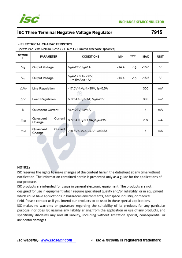
ELECTRICAL CHARACTERISTICS
Tj=25℃ (Vi= -23V, IO=0.5A, Ci= 2.2μF, CO= 1μF unless otherwise specified) SYMBO L PARAMETER CONDITIONS MIN TYP MAX VO Output Voltage VO Output Voltage Vin=-23V; IO=1A Vin=-17.5 to -30V; IO= 5mA to 1A; -14.4 -15 -15.6 -14.4 -15 -15.6 △VV Line Regulation -17.5V≤Vin≤-30V; IO=0.5A 300 UNIT V V mV △Vi Load Regulation...