AD149
Description
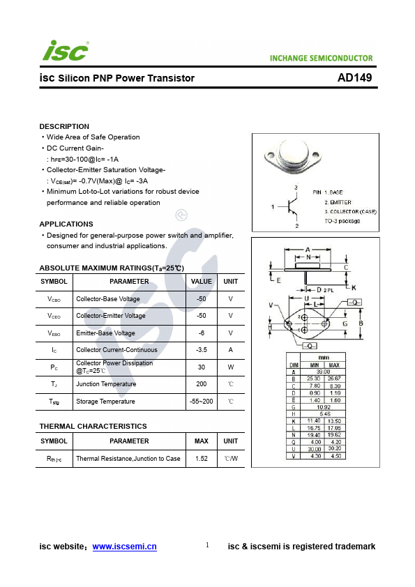
Wide Area of Safe Operation DC Current Gain- : hFE=30-100@IC= -1A Collector-Emitter Saturation Voltage- : VCE(sat)= -0.7V(Max)@ IC= -3A Minimum Lot-to-Lot variations for robust device performance and reliable operation.
Wide Area of Safe Operation DC Current Gain- : hFE=30-100@IC= -1A Collector-Emitter Saturation Voltage- : VCE(sat)= -0.7V(Max)@ IC= -3A Minimum Lot-to-Lot variations for robust device performance and reliable operation.
| Part Number | Manufacturer | Description |
|---|---|---|
| AD142 | Unknown Manufacturer | PNP Transistor |
| AD14BD300 | UNIVERSAL MICROELECTRONICS | Active Delay Lines |
| AD14BD450 | UNIVERSAL MICROELECTRONICS | Active Delay Lines |
| AD14BD400 | UNIVERSAL MICROELECTRONICS | Active Delay Lines |
| AD14AC440 | UNIVERSAL MICROELECTRONICS | Active Delay Lines |
| AD14AC340 | UNIVERSAL MICROELECTRONICS | Active Delay Lines |
| AD14AB150 | UNIVERSAL MICROELECTRONICS | Active Delay Lines |
| AD14AB090 | UNIVERSAL MICROELECTRONICS | Active Delay Lines |
| AD14AB075 | UNIVERSAL MICROELECTRONICS | Active Delay Lines |
| AD14AB060 | UNIVERSAL MICROELECTRONICS | Active Delay Lines |