Datasheet4U.com
🌙
AOTF256L Datasheet | Inchange Semiconductor
Part:
AOTF256L
Description:
N-Channel MOSFET
Category:
MOSFET
Manufacturer:
Inchange Semiconductor
Size:
245.78 KB
AOTF256L Datasheet (PDF) Download
Related AOTF256L Datasheets
AOTF25S65L N-Channel MOSFET
AOTF25S65 N-Channel MOSFET
Inchange Semiconductor
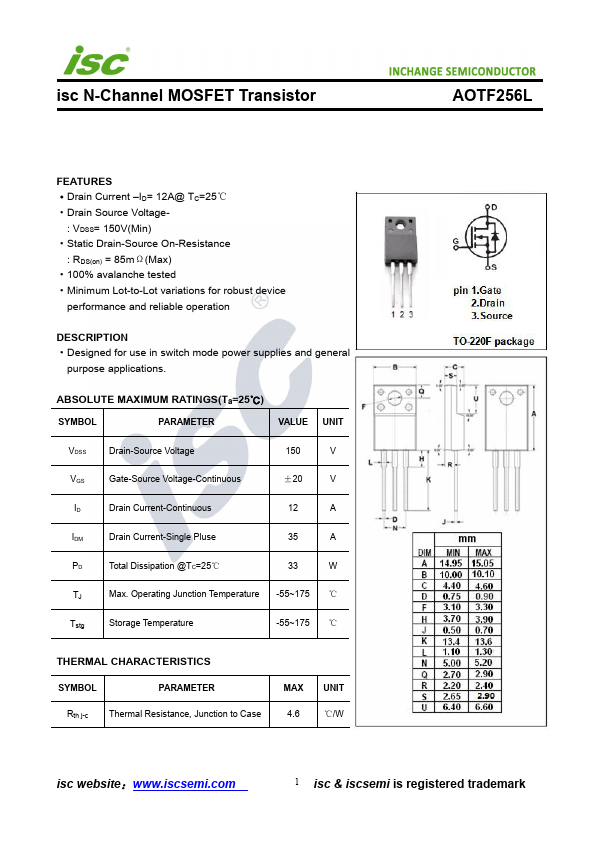
AOTF256L
Description
.
Key Features
Drain Current –ID= 12A@ TC=25℃
Drain Source Voltage
Static Drain-Source On-Resistance
100% avalanche tested
Minimum Lot-to-Lot variations for robust device
×
Close