BUK454-200B
BUK454-200B is N-Channel MOSFET manufactured by Inchange Semiconductor.
- Part of the BUK454-200A comparator family.
- Part of the BUK454-200A comparator family.
DESCRIPTION
- Drain Source Voltage-
: VDSS=200V(Min)
- Low RDS(ON)
- Fast Switching Speed
- Minimum Lot-to-Lot variations for robust device performance and reliable operation
APPLICATIONS
- Designed for Switched Mode Power Supplies (SMPS), motor control,welding, and in general purpose switching resistance application
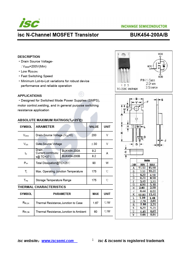
ABSOLUTE MAXIMUM RATINGS(Ta=25℃) SYMBOL ARAMETER
VALUE UNIT
VDSS
Drain-Source Voltage (VGS=0)
Gate-Source Voltage
Drain
BUK454-200A
Current-continuou s@ TC=37℃
Ptot
Total Dissipation@TC=25℃
±30
9.2 A
Tj
Max. Operating Junction Temperature
℃
Tstg
Storage Temperature Range
THERMAL CHARACTERISTICS
SYMBOL
PARAMETER
℃
MAX UNIT
Rth j-c Thermal Resistance,Junction to Case
1.67 ℃/W
Rth j-a Thermal Resistance,Junction to...