SPW15N60C3 Overview
Key Specifications
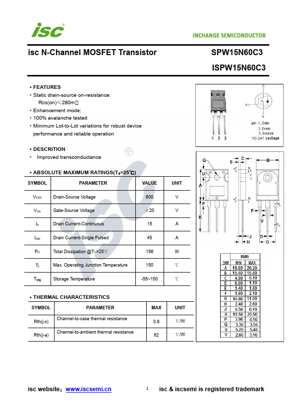
Package: TO-247
Mount Type: Through Hole
Pins: 3
Max Operating Temp: 150 °C
Key Features
- Static drain-source on-resistance: RDS(on)≤280mΩ
- Enhancement mode
- 100% avalanche tested
- Minimum Lot-to-Lot variations for robust device performance and reliable operation
- Improved transconductance