SPW16N50C3 Overview
Key Specifications
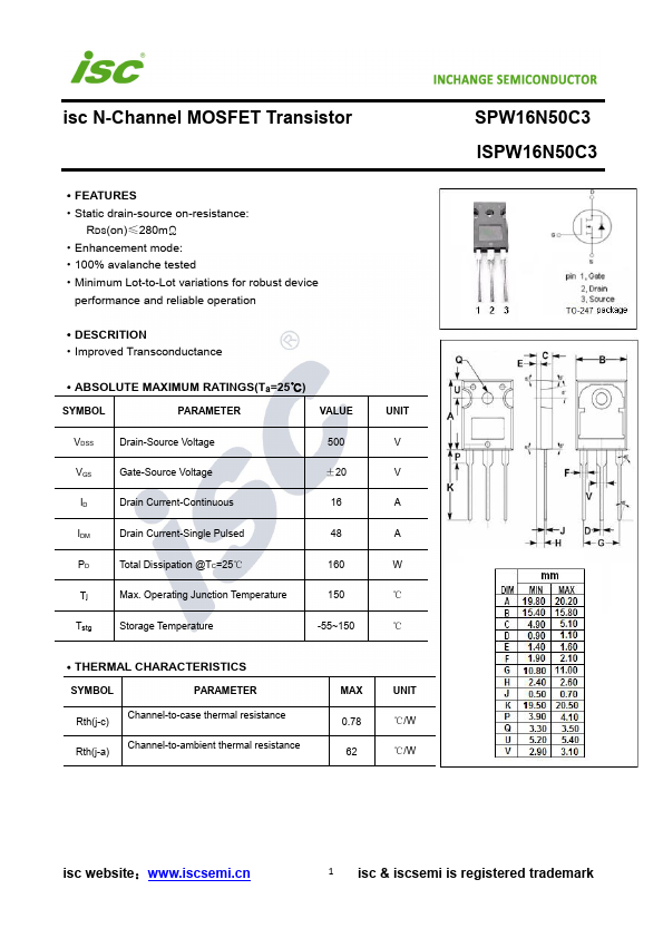
Package: TO-247-3
Pins: 3
Height: 21.1 mm
Length: 16.13 mm
Key Features
- Static drain-source on-resistance: RDS(on)≤280mΩ
- Enhancement mode
- 100% avalanche tested
- Minimum Lot-to-Lot variations for robust device performance and reliable operation
- Improved Transconductance