SPW20N60CFD Overview
Key Specifications
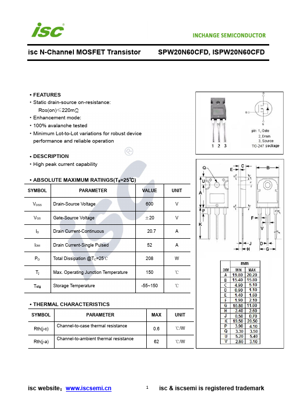
Package: TO-247
Mount Type: Through Hole
Pins: 3
Max Operating Temp: 150 °C
Description
High peak current capability - SYMBOL PARAMETER VALUE VDSS Drain-Source Voltage 600 VGS Gate-Source Voltage ±20 ID Drain Current-Continuous 20.7 IDM Drain Current-Single Pulsed 52 PD Total Dissipation @TC=25℃ 208 Tj Max. Operating Junction Temperature 150 Tstg Storage Temperature -55~150 UNIT V V A A W ℃ ℃ - SYMBOL PARAMETER Rth(j-c) Channel-to-case Rth(j-a) Channel-to-ambient MAX 0.6 62 UNIT ℃/W ℃/W isc website: 1 isc & iscsemi is registered trademark isc N-Channel MOSFET Transistor SPW20N60CFD, ISPW20N60CFD TC=25℃ unless otherwise specified SYMBOL PARAMETER CONDITIONS MIN TYP MAX UNIT BVDSS Drain-Source Breakdown Voltage VGS=0V; ID=0.25mA 600 V VGS(th) Gate Threshold Voltage VDS=VGS; ID=1mA 3 5 V RDS(on) Drain-Source On-Resistance VGS=10V; ID=13.1A 220 mΩ IGSS Gate-Source Leakage Current VGS= 20V; VDS= 0V 0.1 μA IDSS Drain-Source Leakage Current VDS=600V; VGS= 0V 2.1 μA VSD Diode forward voltage IF=IS, VGS = 0V 1.2 V trr Reverse Recovery Time 300 ns VR=480V;IF=IS; diF/dt = 100A/µs Qrr Reverse Recovery Charge 5 µC NOTICE: ISC reserves the rights to make changes of the content herein the datasheet at any time without notification.
Key Features
- Static drain-source on-resistance: RDS(on)≤220mΩ
- Enhancement mode
- 100% avalanche tested
- Minimum Lot-to-Lot variations for robust device performance and reliable operation