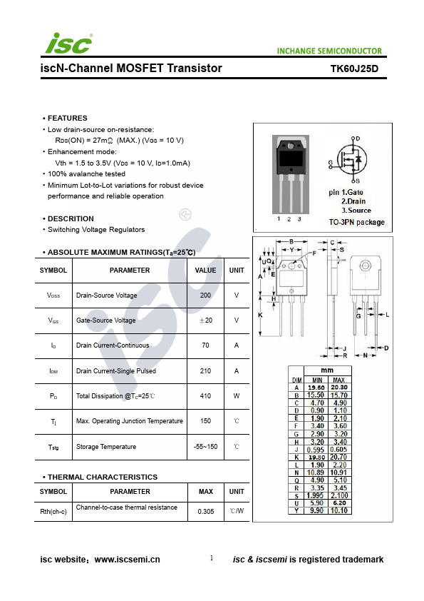
TK60J25D
TK60J25D is N-Channel MOSFET manufactured by Inchange Semiconductor.
FEATURES
- Low drain-source on-resistance:
RDS(ON) = 27mΩ (MAX.) (VGS = 10 V)
- Enhancement mode:
Vth = 1.5 to 3.5V (VDS = 10 V, ID=1.0m A)
- 100% avalanche tested
- Minimum Lot-to-Lot variations for robust device performance and reliable operation
- DESCRITION
- Switching Voltage Regulators
- ABSOLUTE MAXIMUM RATINGS(Ta=25℃)
SYMBOL
PARAMETER
VALUE
UNIT
VDSS
Drain-Source Voltage
Gate-Source Voltage
±20
Drain Current-Continuous
Drain Current-Single Pulsed
Total Dissipation @TC=25℃
Tj
Max. Operating Junction Temperature
℃
Tstg
Storage Temperature
-55~150 ℃
- THERMAL CHARACTERISTICS
SYMBOL
PARAMETER...