NJ30
NJ30 is Silicon Junction Field-Effect Transistor Low-Noise High Gain Amplifier manufactured by INTERFET.
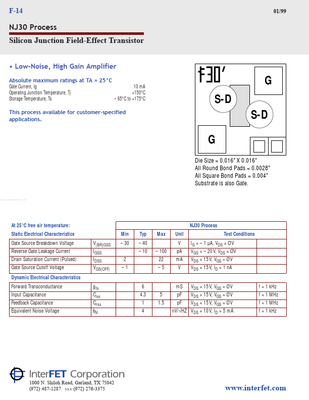
F-14
01/99
NJ30 Process
Silicon Junction Field-Effect Transistor
- Low-Noise, High Gain...
| Manufacturer | Part Number | Description |
|---|---|---|
| NJ301-1100 | Machine Automation Controller | |
| NJ301-1200 | Machine Automation Controller |