IPS FSW25N50A
N-Channel MOSFET
| Part No. | FSW25N50A |
|---|---|
| Datasheet | FSW25N50A Download |
| Manufacturer |  IPS |
| Description | N-Channel MOSFET |
| Buy | Stock & Price |
APPLICATIONS
:● Uninterruptible Power Supply(UPS)
● LCD Panel Power
● SMPS Power
● DC-AC Inverter FSW25N50
● RoHS Compliant
● Low ON Resistance
● Low Gate Charge
● Peak Current vs Pulse Width Curve
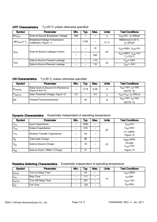
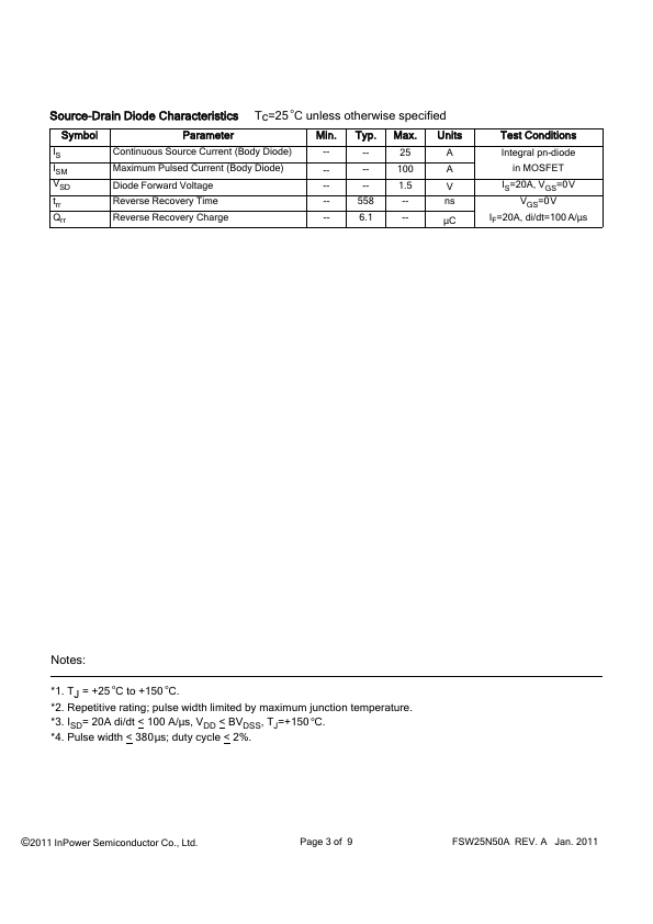
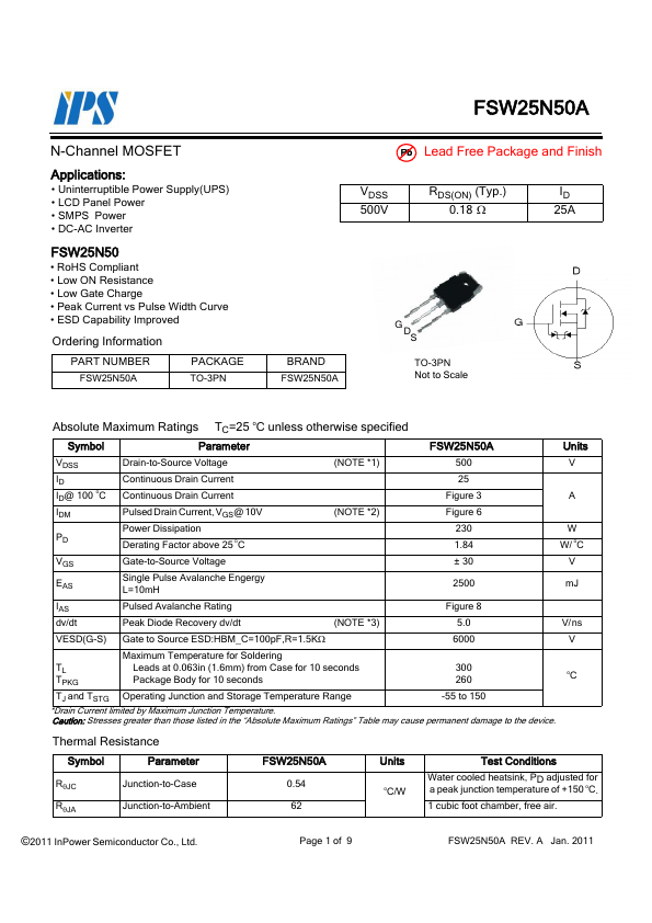
● ESD Capability Improved Ordering Information PART NUMBER FSW25N50A PACKAGE TO-3PN FSW25N50A Pb Lead Free Package and Finish VDSS RDS(ON) (Typ.) ID 500V 0.18 : 25A BRAND FSW25N50A G DS TO-3PN Not to Scale
ABSOLUTE MAXIMUM RATINGS
TC=25 oC unless otherwise specified Symbol Parameter FSW25N50A Units VDSS ID ID@ 100 oC IDM PD Drain-to-Source Voltage Continuous Drain Current Continuous Drain Current Pulsed Drain Current, VGS@ 10V Power Dissipation Derating Factor above 25 oC (NOTE *1) (NOTE *2) 500 25 Figure 3 Figure 6 230 1.84 V A W W/ oC VGS Gate-to-Source Voltage EAS Single Pulse Avalanche Engergy L=10mH ± 30 V 2500 mJ IAS dv/dt Pulsed Avalanche Rating Peak Diode Recovery dv/dt (NOTE *3) Figure 8 5.0 V/ ns VESD(G-S) Gate to Source ESD:HBM_C=100pF,R=1.5K: 6000 V Maximum Temperature for Solder...