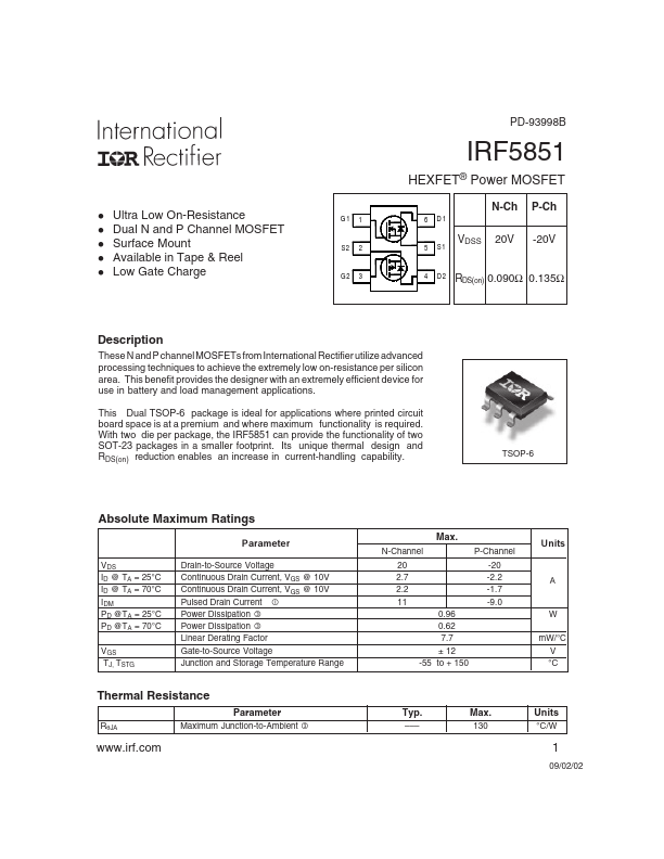
DESCRIPTION
These N and P channel MOSFETs from International Rectifier utilize advanced processing techniques to achieve the extremely low on-resistance per silicon area. This benefit provides the designer with an extremely efficient device for use in battery and load management applications. This Dual TSOP-6 package is ideal for applications where printed circuit board space is at a premium and where maximum functionality is required. With two die per package, TSOP-6 ABSOLUTE MAXIMUM RATINGS
Parameter VDS ID @ TA = 25°C ID @ TA = 70°C IDM PD @TA = 25°C PD @TA = 70°C VGS TJ, TSTG Drain-to-Source Voltage Continuous Drain Current, VGS @ 10V Continuous Drain Current, VGS @ 10V Pulsed Drain Current Power Dissipation Power Dissipation Linear Derating Factor Gate-to-Source Voltage Junction and Storage Temperature Range Thermal Resistance Parameter RθJA Maximum Junction-to-Ambient Max. N-Channel P-Channel 20 -20 2.7 -2.2 2.2 -1.7 11 -9.0 0.96 0.62 7.7 ± 12 -55 to + 150 Units A W mW/°C V °C Typ. ––– Max. International Rectifier