APPLICATIONS
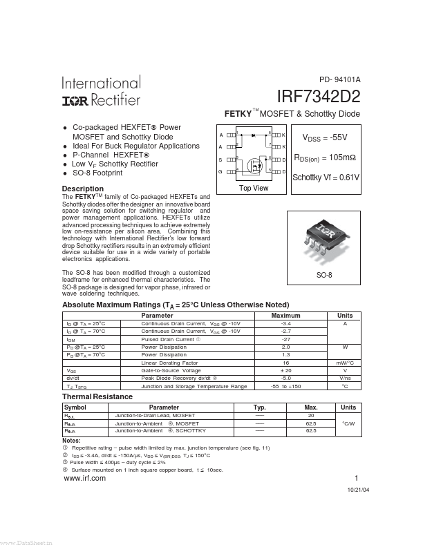
P-Channel HEXFET® Low VF Schottky Rectifier SO-8 Footprint A A S G 1 8 K K D D VDSS = -55V RDS(on) = 105mΩ Schottky Vf = 0.61V 2 7 3 6 4 5 DESCRIPTION
HEXFETs utilize advanced processing techniques to achieve extremely low on-resistance per silicon area. Combining this technology with International Rectifier's low forward drop Schottky rectifiers results in an extremely efficient device suitable for use in a wide variety of portable electronics applications. The SO-8 package is designed for vapor phase, infrared or wave soldering techniques. Top View SO-8 ABSOLUTE MAXIMUM RATINGS
(TA = 25°C Unless Otherwise Noted) Parameter ID @ TA = 25°C ID @ TA = 70°C IDM PD @TA = 25°C PD @TA = 70°C VGS dv/dt TJ, TSTG Continuous Drain Current, VGS @ -10V Continuous Drain Current, VGS @ -10V Pulsed Drain Current À Power Dissipation Power Dissipation Linear Derating Factor Gate-to-Source Voltage Peak Diode Recovery dv/dt Á Junction and Storage Temperature Range Maximum -3.4 -2.7 -27 2.0 1. International Rectifier