DESCRIPTION
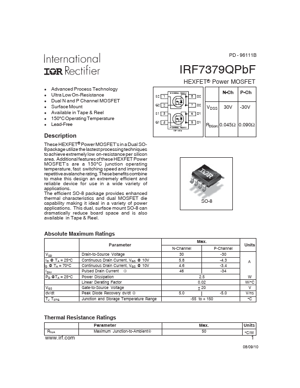
These HEXFET® Power MOSFET's in a Dual SO8 package utilize the lastest processing techniques to achieve extremely low on-resistance per silicon area. Additional features of these HEXFET Power MOSFET's are a 150°C junction operating temperature, fast switching speed and improved repetitive avalanche rating. These benefits combine to make this design an extremely efficient and reliable device for use in a wide variety of applications. S2 1 G2 2 S1 3 G1 4 PD - 96111B IRF7379QPbF HEXFET® Power MOSFET 8 D2 N-Ch P-Ch 7 D2 6 D1 VDSS 30V -30V 5 D1 RDS(on) 0.045Ω 0.090Ω SO-8 ABSOLUTE MAXIMUM RATINGS
VSD ID @ TA = 25°C ID @ TA = 70°C IDM PD @TA = 25°C VGS dv/dt TJ, TSTG Parameter Drain-to-Source Voltage Continuous Drain Current, VGS @ 10V Continuous Drain Current, VGS @ 10V Pulsed Drain Current Power Dissipation Linear Derating Factor Gate-to-Source Voltage Peak Diode Recovery dv/dt Junction and Storage Temperature Range Max. N-Channel P-Channel 30 -30 5.8 -4.3 4.6 -3.4 46 -34 2.5 0.02 ± 20 5.0 -5.0 -55 to + 150 Units A W W/°C V V/ns °C Thermal Resistance Ratings RθJA Parameter Maximum Junction-to-Ambient Max. International Rectifier