IS46R16160D Overview
Key Specifications
Package: TSSOP
Pins: 66
Operating Voltage: 2.5 V
Max Voltage (typical range): 2.7 V
Key Features
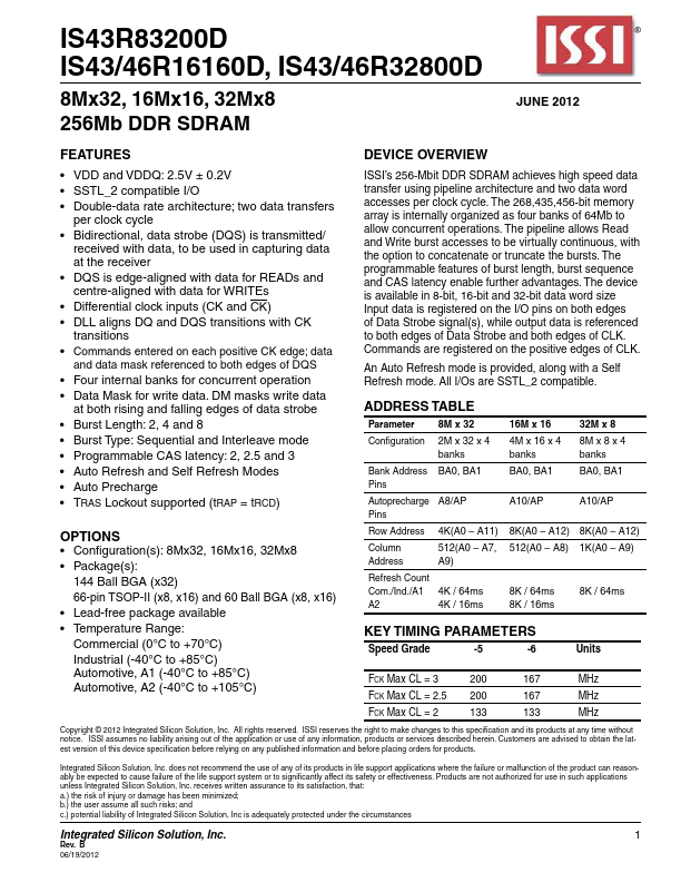
- VDD and VDDQ: 2.5V ± 0.2V
- SSTL_2 compatible I/O
- Double-data rate architecture; two data transfers per clock cycle
- Bidirectional, data strobe (DQS) is transmitted/ received with data, to be used in capturing data at the receiver
- DQS is edge-aligned with data for READs and centre-aligned with data for WRITEs

