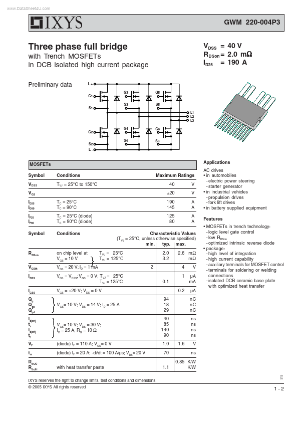
GWM220-004P3
Key Features
- MOSFETs in trench technology: - logic level gate control - low RDSon - optimized intrinsic reverse diode
- package: - high level of integration - high current capability - auxiliary terminals for MOSFET control - terminals for soldering or welding connections - isolated DCB ceramic base plate with optimized heat transfer Characteristic Values (TVJ = 25°C, unless otherwise specified) min. typ. max. TVJ = 25°C TVJ = 125°C 2 0.1 0.2 94 18 29 40 85 140 90 1.0 70 1.1 1.6 2.0 3.2 2.6 m Ω mΩ 4 1 V µA mA µA nC nC nC ns ns ns ns V ns 0.85 K/W K/W RDSon VGSth IDSS IGSS Qg Qgs Qgd td(on) tr td(off) tf VF t rr RthJC RthJH on chip level at VGS = 10 V VDS = 20 V; ID = 1 mA VDS = VDSS; VGS = 0 V; TVJ = 25°C TVJ = 125°C VGS = ±20 V; VDS = 0 V VGS= 10 V; VDS = 14 V; ID = 25 A VGS= 10 V; VDS = 30 V; ID = 25 A; RG = 10 Ω (diode) IF = 110 A; VGS= 0 V (diode) IF = 20 A; -di/dt = 100 A/µs; VDS= 20 V with heat transfer paste IXYS reserves the right to change limits, test conditions and dimensions. © 2005 IXYS All rights reserved 1-2 515