Datasheet4U Logo Datasheet4U.com

IXTA182N055T7 - Power MOSFET

Features

  • Ultra-low On Resistance Unclamped Inductive Switching (UIS) g rated Low package inductance - easy to drive and to protect 175 ° C Operating Temperature Symbol Test Conditions (TJ = 25° C unless otherwise specified) BVDSS VGS = 0 V, ID = 250 µA VGS(th) VDS = VGS, ID = 250 µA IGSS VGS = ± 20 V, VDS = 0 V IDSS VDS = VDSS VGS = 0 V TJ = 150° C RDS(on) VGS = 10 V, ID = 25 A, Note 1 Characteristic Values Min. Typ. Max. 55 V 2.0 4.0 V ± 100 nA 5 µA 250 µA 3.5 5.0 m Ω Advantages Easy.

📥 Download Datasheet

Datasheet preview – IXTA182N055T7
Other Datasheets by IXYS Corporation

Full PDF Text Transcription

Click to expand full text
Preliminary Technical Information TrenchMVTM IXTA182N055T7 Power MOSFET N-Channel Enhancement Mode Avalanche Rated VDSS = ID25 = RDS(on) ≤ 55 182 5.0 V A mΩ Symbol VDSS VDGR VGSM ID25 ILRMS IDM IAR EAS dv/dt PD TJ TJM Tstg TL TSOLD Weight Test Conditions TJ = 25° C to 175° C TJ = 25° C to 175° C; RGS = 1 MΩ Transient TC = 25° C Package Current Limit, RMS TC = 25° C, pulse width limited by TJM TC = 25° C TC = 25° C IS ≤IDM, di/dt ≤100 A/µs, VDD ≤VDSS TJ ≤175° C, RG = 5 Ω TC = 25° C 1.6 mm (0.062 in.) from case for 10 s Plastic body for 10 seconds 
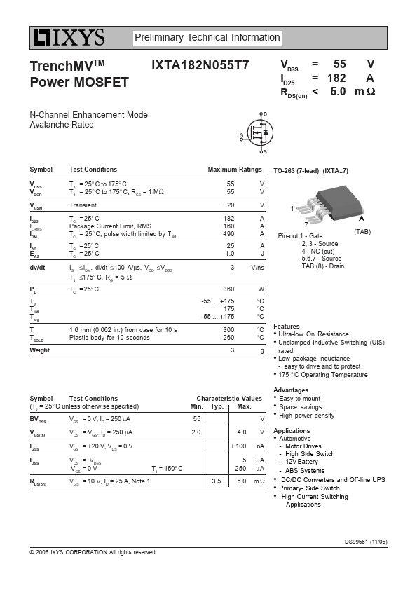
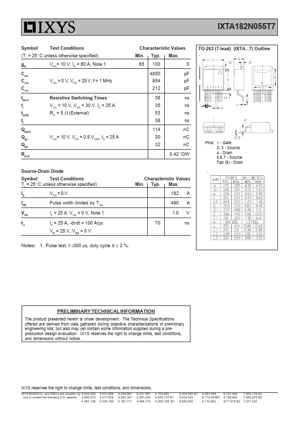
Maximum Ratings TO-263 (7-lead) (IXTA..7) 55 V 55 V ± 20 182 160 490 25 1.0 3 V A A A A J V/ns 1 7 Pin-out:1 - Gate 2, 3 - Source 4 - NC (cut) 5,6,7 - Source TAB (8) - Drain (TAB) 360 -55 ... +175 175 -55 ...
Published: |