IXTC13N50
Features
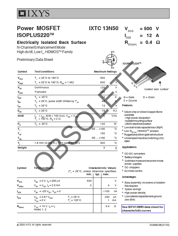
D = Drain z Silicon chip on Direct-Copper-Bond substrate
- High power dissipation
- Isolated mounting surface
- 2500V electrical isolation z Lowdraintotabcapacitance(<35p F) z Low RDS (on) HDMOSTM process z Ruggedpolysilicongatecellstructure z Unclamped Inductive Switching(UIS) rated
Applications z DC-DC converters z Batterychargers z Switched-modeandresonant-mode power supplies z DC choppers z AC motor control min. typ. max.
Advantages
VGS = 0 V, ID = 250 µA VDS = VGS, ID = 2.5 m A
VGS = ±20 VDC, VDS = 0
V z Easy assembly: no screws or isolation
4V foils required
±100 n A z Space savings z High power density
VDS = 0.8
- VDSS VGS = 0 V
TJ = 25°C TJ = 125°C
200 µA 1 m A z Lowcollectorcapacitancetoground (low EMI)
RDS(on)
NVGo Ste=s
10 V, 1, 2
=
0.4 Ω
See IXFH13N50 data sheet for characteristic curves
© 2003 IXYS All rights reserved
DS98823B(07/03)
IXTC 13N50
Symbol
Test Conditions
Characteristic Values
(TJ = 25°C, unless otherwise...