P5N50 Overview
Key Specifications
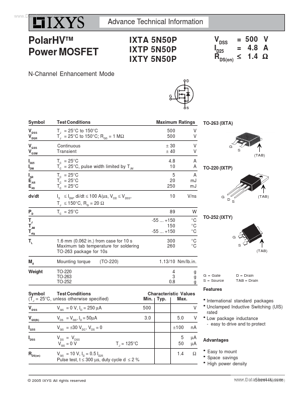
Package: TO-220AB
Mount Type: Through Hole
Pins: 3
Height: 19.89 mm
Key Features
- International standard packages Unclamped Inductive Switching (UIS) rated Low package inductance
- easy to drive and to protect Advantages z z