DESCRIPTION
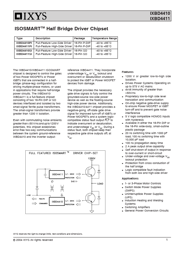
Package Temperature Range IXBD4410PI IXBD4411PI IXBD4410SI IXBD4411SI Full-Feature Low-Side Driver 16-Pin P-DIP Full-Feature High-Side Driver 16-Pin P-DIP Full-Feature Low-Side Driver 16-Pin SO Full-Feature High-Side Driver 16-Pin SO -40 to +85°C -40 to +85°C -40 to +85°C -40 to +85°C Even with commutating noise ambients greater than ±50 V/ns and up to 1200 V potentials, this chipset establishes error-free two-way communications between the system ground-reference IXBD4410 and the inverter output- reference IXBD4411. They incorporate undervoltage VDD or VEE lockout and overcurrent or desaturation shutdown to protect the IGBT or Power MOSFET devices from damage. The chipset provides the necessary gate drive signals to fully control the grounded-source low-side power device as well as the floating-source high-side power device. Additionally, the IXBD4410/4411 chipset provides a negative-going, off-state gate drive signal for improved turn-off of IGBTs or Power MOSFETs and a system logiccompatible status fault output FLT to indicate overcurrent or desaturation, and undervoltage VDD or VEE. IXYS