IXTQ88N28T Description
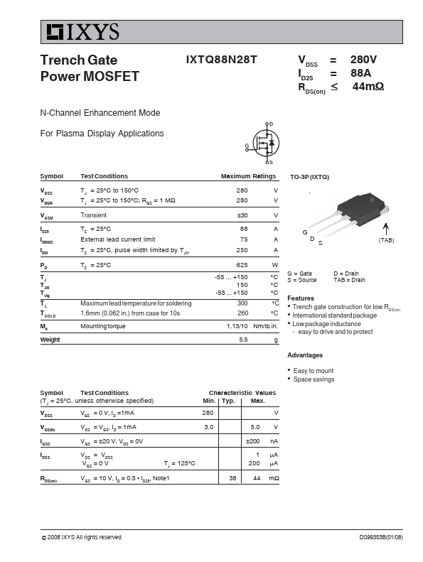
+150 °C 300 °C 260 °C 1.13/10 Nm/lb.in. 5.5 g G = Gate S = Source D = Drain TAB = Drain.
IXTQ88N28T Key Features
- easy to drive and to protect
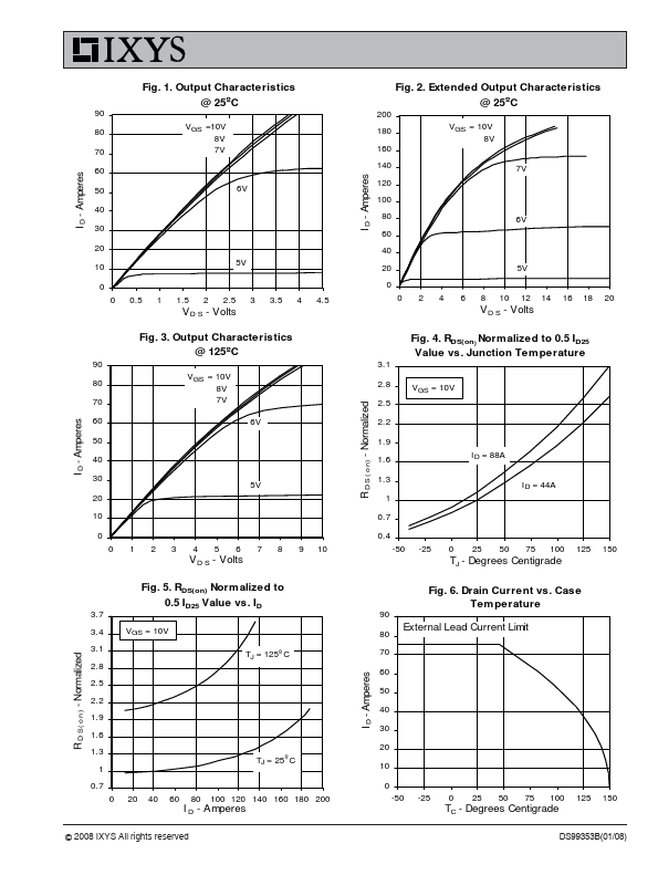
- ID25, Note1
- VDSS, ID = 0.5
- di/dt = 100 A/μs
- Amperes
- Amperes
- Normalized
IXTQ88N28T is Power MOSFET manufactured by IXYS.
| Manufacturer | Part Number | Description |
|---|---|---|
| IXTQ88N28T | N-Channel MOSFET |
+150 °C 300 °C 260 °C 1.13/10 Nm/lb.in. 5.5 g G = Gate S = Source D = Drain TAB = Drain.