IXYS T0900AF65E
Insulated Gate Bi-Polar Transistor
| Part No. | T0900AF65E |
|---|---|
| Datasheet | T0900AF65E Download |
| Manufacturer |  IXYS |
| Description | Insulated Gate Bi-Polar Transistor |
| Buy | Stock & Price |

ABSOLUTE MAXIMUM RATINGS
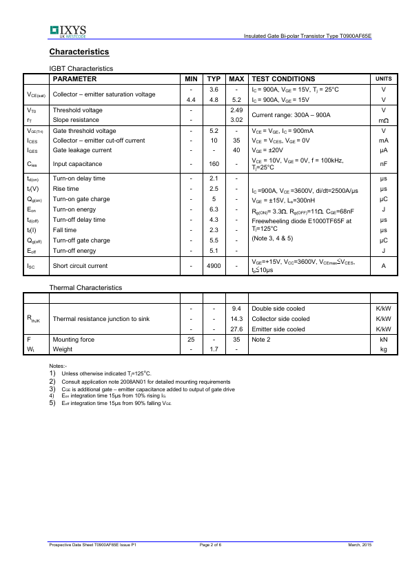
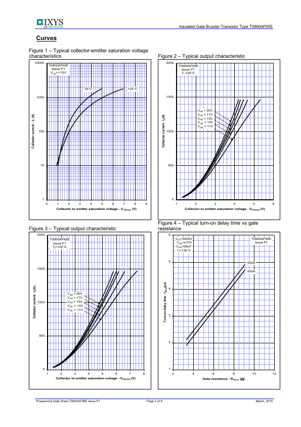
VCES VCES VCES VDC link VGES VOLTAGE RATINGS Collector – emitter voltage Collector – emitter voltage (Tj 25°C) Collector – emitter voltage (Tj -40°C) Permanent DC voltage for 100 FIT failure rate. Peak gate – emitter voltage MAXIMUM LIMITS 6500 6500 6000 3600 ±20 UNITS V V V V V IC ICRM ICEO PMAX Tj Tstg RATINGS DC collector current, IGBT Repetitive peak collector current, tp=1ms, IGBT Maximum reverse emitter current, tp=100µs, (note 2 & 3) Maximum power dissipation, IGBT (Note 2) Operating temperature range. Storage temperature range. Notes: 1) Unless otherwise indicated Tj = 125ºC. 2) Tsink = 25°C, double side cooled. 3) Maximum commutation loop inductance 300nH. MAXIMUM LIMITS 900 1800 900 10.6 -40 to +125 -40 to +125 UNITS A A A KW °C °C Prospective Data Sheet T0900AF65E Issue P1 Page 1 of 6 March, 2015 Characteristics IGBT Characteristics PARAMETER VCE(sat) Collector – emitter saturation voltage VT0 rT VGE(TH) ICES IGES Cies td(on) tr(V) Qg(on) Eon td(off)...