2N3239 Overview
Key Specifications
Description
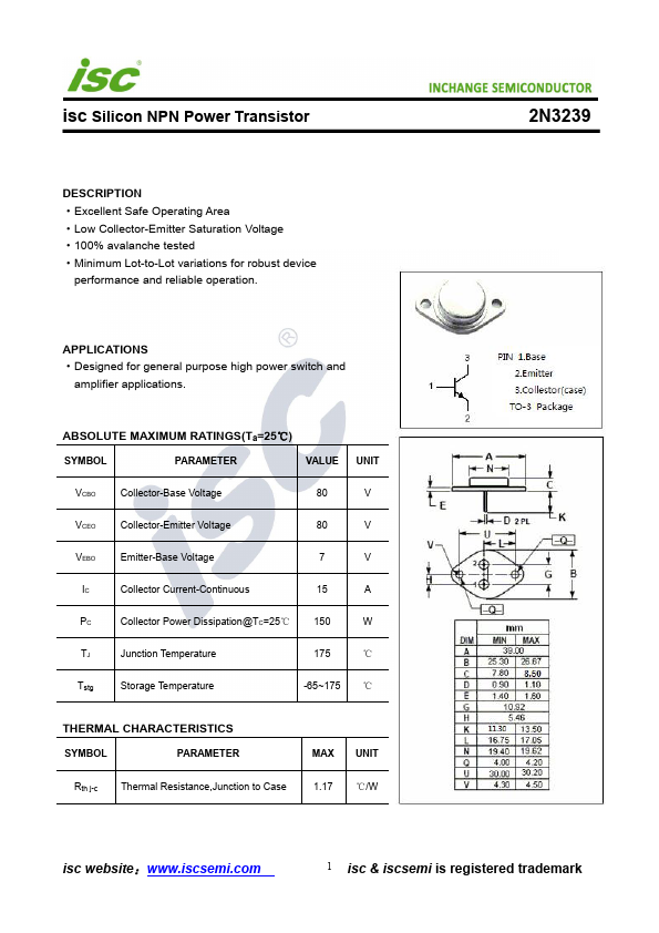
Excellent Safe Operating Area - Low Collector-Emitter Saturation Voltage - 100% avalanche tested - Minimum Lot-to-Lot variations for robust device performance and reliable operation.
| Part | 2N3239 |
|---|---|
| Description | Silicon NPN Power Transistor |
| Category | Transistor |
| Manufacturer | Inchange Semiconductor |
| Size | 170.99 KB |
Excellent Safe Operating Area - Low Collector-Emitter Saturation Voltage - 100% avalanche tested - Minimum Lot-to-Lot variations for robust device performance and reliable operation.
| Seller | Inventory | Price Breaks | Buy |
|---|---|---|---|
| No distributor offers were returned for this part. | |||
| Part Number | Manufacturer | Description |
|---|---|---|
| 2N3237 | SavantIC | Silicon NPN Power Transistors |
| 2N3235 | Westinghouse | Silicon Power Transistors |
| 2N3232 | SavantIC | Silicon NPN Power Transistors |
| 2N3235 | Motorola Semiconductor | NPN silicon power transistors |
| 2N323 | Motorola Semiconductor | PNP Transistor |