BSP615S2L
BSP615S2L is OptiMOS Power-Transistor manufactured by Infineon.
BSP615S2L OptiMOS Power-Transistor
Feature
- N-Channel
Product Summary VDS R DS(on) ID 55 90 2.8
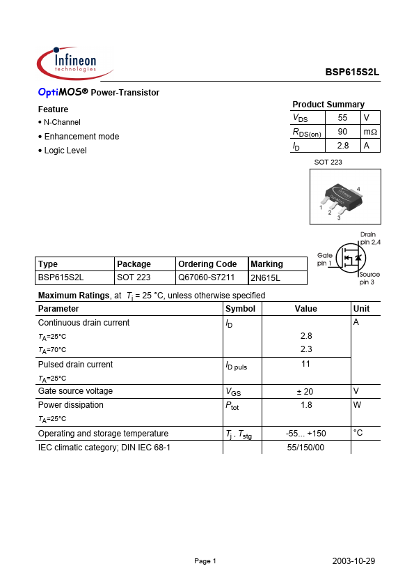
SOT 223
V mΩ A
- Enhancement mode
- Logic Level
Type BSP615S2L
Package SOT 223
Ordering Code Q67060-S7211
Marking 2N615L
Maximum Ratings, at Tj = 25 °C, unless otherwise specified Parameter Continuous drain current
TA=25°C TA=70°C
Symbol ID
Value 2.8 2.3
Unit A
Pulsed drain current
TA=25°C
ID puls VGS Ptot Tj , Tstg
11 ± 20 1.8 -55... +150 55/150/00 V W °C
Gate source voltage Power dissipation
TA=25°C
Operating and storage temperature IEC climatic category; DIN IEC 68-1
Page 1
2003-10-29
Thermal Characteristics Parameter Characteristics Thermal resistance, junction...