SEMB3
SEMB3 is PNP Silicon Digital Transistor Preliminary data manufactured by Infineon.
PNP Silicon Digital Transistor Preliminary data
- Switching circuit, inverter, interface circuit, driver circuit
- Two ( galvanic) internal isolated Transistors with good matching in one package
- Built in bias resistor ( R1 = 4.7kΩ)
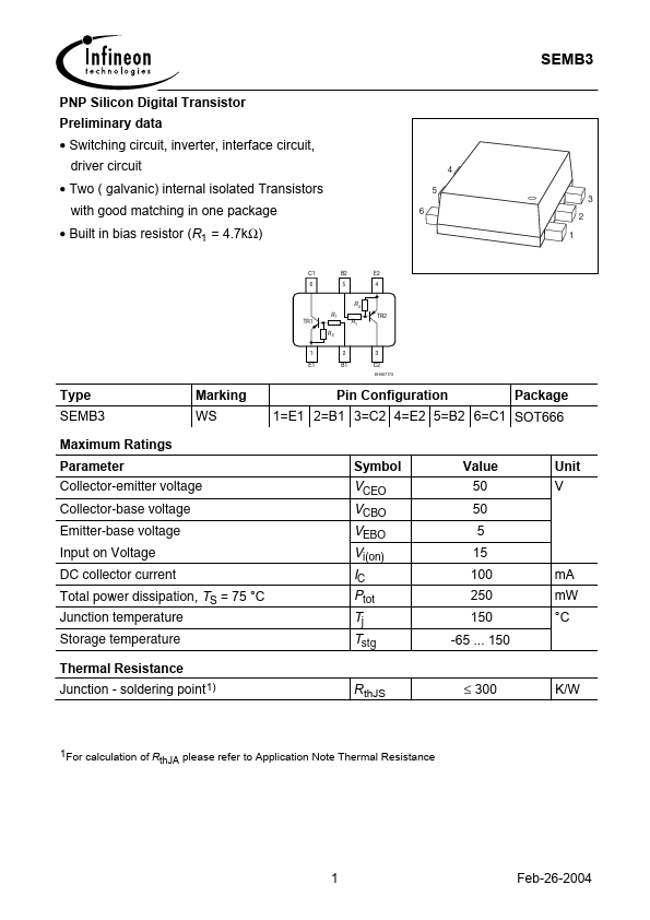
C1 6 B2 5 E2 4
4 5 3 6 1 2
R2 R1 TR1 R2 1 E1 2 B1 3 C2
EHA07173
TR2 R1
Type SEMB3
Maximum Ratings Parameter
Marking WS
Pin Configuration Package 1=E1 2=B1 3=C2 4=E2 5=B2 6=C1 SOT666
Symbol VCEO VCBO VEBO Vi(on) IC Ptot Tj Tstg
Value 50 50 5 15 100 250 150 -65 ... 150
Unit V
Collector-emitter voltage Collector-base voltage Emitter-base voltage Input on Voltage DC collector current Total power dissipation, TS = 75 °C Junction temperature Storage temperature
Thermal Resistance m A m W °C
Junction
- soldering point 1)
Rth JS
≤ 300
K/W
1For calculation of R th JA please refer to Application Note Thermal Resistance
Feb-26-2004
Electrical Characteristics at TA=25°C, unless otherwise specified Symbol Values Parameter min. DC Characteristics Collector-emitter breakdown voltage IC = 100 µA, IB = 0 Collector-base breakdown voltage IC = 10 µA, IE = 0 Emitter-base breakdown voltage IE = 10 µA, IC = 0 Collector cutoff current VCB = 40 V, IE = 0 DC current gain 1) IC = 5 m A, VCE = 5 V Collector-emitter saturation voltage1) IC = 10 m A, IB = 0.5 m A Input off voltage IC = 100 µA, VCE = 5 V Input on Voltage IC = 2 m A, VCE = 0.3 V Input resistor
AC Characteristics Transition frequency IC = 10 m A, VCE = 5 V, f = 100 MHz Collector-base capacitance VCB = 10 V, f = 1 MHz Ccb 3 f T 200
- Unit max. 100 630 0.3 0.8 1.1 6.2 kΩ
MHz p F typ. 4.7
V(BR)CEO V(BR)CBO V(BR)EBO ICBO h FE VCEsat Vi(off) Vi(on) R1
50 50 5 120 0.4 0.5 3.2
V n A V
1) Pulse test: t < 300µs; D < 2%
Feb-26-2004
DC Current Gain h FE = f (I C) VCE = 5V (mon emitter configuration)
10 3
Collector-Emitter Saturation Voltage VCEsat = f (IC), h FE = 20
10...