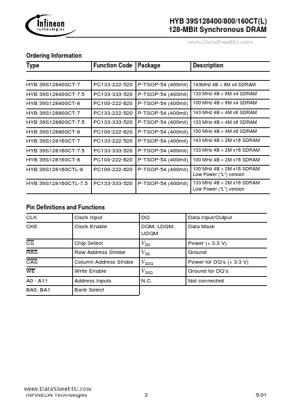
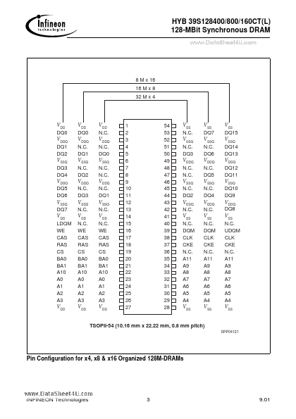
HYB39S128400CT Datasheet Text
HYB 39S128400/800/160CT(L) 128-MBit Synchronous DRAM
..
128-MBit Synchronous DRAM
- High Performance: -7 -7.5 133 7.5 5.4 10 6 -8 125 8 6 10 6 Units MHz ns ns ns ns
- Multiple Burst Read with Single Write Operation
- Automatic and Controlled Precharge mand
- Data Mask for Read/Write Control (x4, x8)
- Data Mask for byte control (x16)
- Auto Refresh (CBR) and Self Refresh
- Power Down and Clock Suspend Mode
- 4096 Refresh Cycles / 64 ms fCK tCK3 tAC3 tCK2 tAC2
143 7 5.4 7.5 5.4
- Single Pulsed RAS Interface
- Fully Synchronous to Positive Clock Edge
- 0 to 70 °C operating temperature
- Four Banks controlled by BA0 & BA1
- Programmable CAS Latency: 2, 3
- Programmable Wrap Sequence: Sequential or Interleave
- Programmable Burst Length: 1, 2, 4, 8 and full page
- Random Column Address every CLK (1-N Rule)
- Single 3.3 V ± 0.3 V Power Supply
- LVTTL Interface
- Plastic Packages: P-TSOPII-54 400mil x 875 mil width (x4, x8, x16)
- -7 for PC 133 2-2-2 applications -7.5 for PC 133 3-3-3 applications -8 for PC100 2-2-2 applications
The HYB 39S128400/800/160CT are four bank Synchronous DRAM’s organized as 4 banks × 8MBit x4, 4 banks × 4MBit x8 and 4 banks × 2Mbit x16 respectively. These synchronous devices achieve high speed data transfer rates by employing a chip architecture that prefetches multiple bits and then synchronizes the output data to a system clock. The chip is fabricated using the Infineon advanced 0.17 micron process technology. The device is designed to ply with all industry standards set for synchronous DRAM products, both electrically and mechanically. All of the control, address, data input and output circuits are synchronized with the positive edge of an externally supplied clock. Operating the four memory banks in an...