IPB06N03LAG
IPB06N03LAG is Power-Transistor manufactured by Infineon.
Features
- Ideal for high-frequency dc/dc converters
- Qualified according to JEDEC1) for target applications
- N-channel
- Logic level
- Excellent gate charge x R DS(on) product (FOM)
- Very low on-resistance R DS(on)
- Superior thermal resistance
- 175 °C operating temperature
- dv /dt rated
- Pb-free lead plating; Ro HS pliant
Product Summary V DS R DS(on),max (SMD version) ID 25 5.9 50 V mΩ A
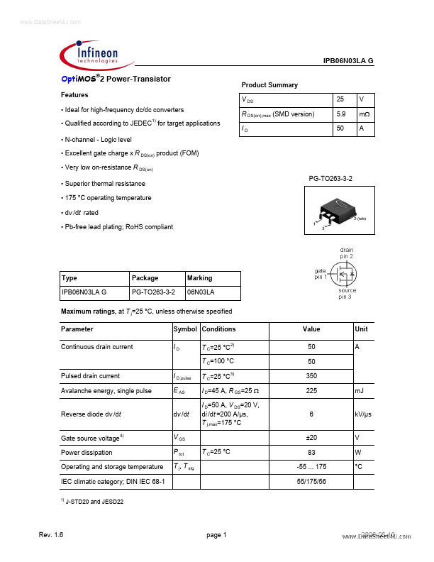
PG-TO263-3-2
Type IPB06N03LA G
Package PG-TO263-3-2
Marking 06N03LA
Maximum ratings, at T j=25 °C, unless otherwise specified Parameter Continuous drain current Symbol Conditions ID T C=25 °C2) T C=100 °C Pulsed drain current Avalanche energy, single pulse Reverse diode d v /dt Gate source voltage4) Power dissipation Operating and storage temperature IEC climatic category; DIN IEC 68-1
1)
Value 50 50 350 225 6 ±20
Unit A
I D,pulse E AS dv /dt V GS P tot T j, T stg
T C=25 °C3) I D=45 A, R GS=25 Ω I D=50 A, V DS=20 V, di /dt =200 A/µs, T j,max=175 °C m J k V/µs V W °C
T C=25 °C
83 -55 ... 175 55/175/56
J-STD20 and JESD22
Rev. 1.6 page 1
2006-05-10
..
IPB06N03LA G
Parameter Symbol Conditions min. Thermal characteristics Thermal resistance, junction
- case SMD version, device on PCB R th JC R th JA minimal footprint 6 cm2 cooling area5) Electrical characteristics, at T j=25 °C, unless otherwise specified Static characteristics Drain-source breakdown voltage Gate threshold voltage Zero gate voltage drain current V (BR)DSS V GS=0 V, I D=1 m A V GS(th) I DSS V DS=V GS, I D=40 µA V DS=25 V, V GS=0 V, T j=25 °C V DS=25 V, V GS=0 V, T j=125 °C Gate-source leakage current Drain-source on-state resistance I GSS R DS(on) V GS=20 V, V DS=0 V V GS=4.5 V, I D=30 A, SMD version V GS=10 V, I D=30 A, SMD version Gate resistance Transconductance RG g fs |V DS|>2|I D|R DS(on)max, I D=30 A 25 1.2 1.6 0.1 2 1 µA V 1.8 62 40 K/W Values typ. max. Unit
- 10 10 7.6
100 100 9.5 n A mΩ
4.9 1.2 58
5.9 Ω S
2)
Current is limited by bondwire; with an R th JC=1.8 K/W the chip is able...