IPB100N04S3-03
IPB100N04S3-03 is OptiMOS-T Power-Transistor manufactured by Infineon.
tures
- N-channel
- Enhancement mode
- Automotive AEC Q101 qualified
- MSL1 up to 260°C peak reflow
- 175°C operating temperature
- Green package (Ro HS pliant)
- Ultra low Rds(on)
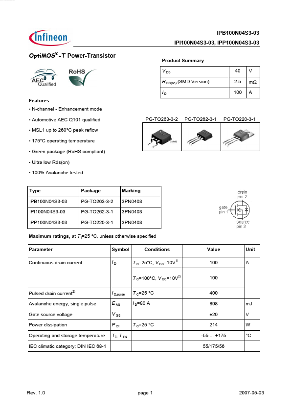
- 100% Avalanche tested PG-TO263-3-2 PG-TO262-3-1 PG-TO220-3-1
Type IPB100N04S3-03 IPI100N04S3-03 IPP100N04S3-03
Package PG-TO263-3-2 PG-TO262-3-1 PG-TO220-3-1
Marking 3PN0403 3PN0403 3PN0403
Maximum ratings, at T j=25 °C, unless otherwise specified Parameter Continuous drain current Symbol ID Conditions T C=25°C, V GS=10V1) T C=100°C, V GS=10V2) Pulsed drain current2) Avalanche energy, single pulse Gate source voltage Power dissipation Operating and storage temperature IEC climatic category; DIN IEC 68-1 I D,pulse E AS V GS P tot T j, T stg T C=25 °C T C=25 °C I D=80 A Value 100 100 400 898 ±20 214 -55 ... +175 55/175/56 m J V W °C Unit A
Rev. 1.0 page 1
2007-05-03
IPB100N04S3-03 IPI100N04S3-03, IPP100N04S3-03
Parameter Symbol Conditions min. Thermal characteristics2) Thermal resistance, junction
- case Thermal resistance, junction ambient, leaded SMD version, device on PCB R th JC R th JA R th JA minimal footprint 6 cm2 cooling area3) Electrical characteristics, at T j=25 °C, unless otherwise specified Static characteristics Drain-source breakdown voltage Gate threshold voltage Zero gate voltage drain current V (BR)DSS V GS=0 V, I D= 1 m A V GS(th) I DSS V DS=V GS, I D=150 µA V DS=40 V, V GS=0 V, T j=25 °C V DS=40 V, V GS=0 V, T j=125 °C2) Gate-source leakage current Drain-source on-state resistance I GSS RDS(on) V GS=20 V, V DS=0 V V GS=10 V, I D=80 A V GS=10 V, I D=80 A, SMD version 40 2.1 3.0 4.0 1 µA V 0.7 62 62 40 K/W Values typ. max. Unit
- 2.2 1.9
100 100 2.8 2.5 n A mΩ
Rev. 1.0 page 2
2007-05-03
IPB100N04S3-03 IPI100N04S3-03, IPP100N04S3-03
Parameter Symbol Conditions min. Dynamic characteristics2) Input capacitance Output capacitance Reverse transfer capacitance Turn-on delay time Rise time Turn-off delay time Fall time Gate Charge Characteristics2) Gate to source...