IPB60R600CP
IPB60R600CP is Power Transistor manufactured by Infineon.
Cool MOSTM Power Transistor
Features
- Lowest figure-of-merit R ON x Qg
- Ultra low gate charge
- Extreme dv/dt rated
- High peak current capability
- Qualified according to JEDEC1) for target applications
- Pb-free lead plating; Ro HS pliant
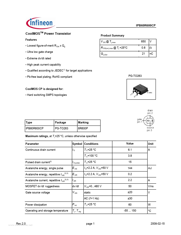
Product Summary V DS @ Tj,max R DS(on),max @ Tj =25°C Q g,typ 650 0.6 21 V Ω n C
PG-TO263
Cool MOS CP is designed for:
- Hard switching SMPS topologies
Type IPB60R600CP
Package PG-TO263
Marking 6R600P
Maximum ratings, at T j=25 °C, unless otherwise specified Parameter Continuous drain current Symbol Conditions ID T C=25 °C T C=100 °C Pulsed drain current2) Avalanche energy, single pulse Avalanche energy, repetitive t AR2),3) Avalanche current, repetitive t AR2),3) MOSFET dv /dt ruggedness Gate source voltage I D,pulse E AS E AR I AR dv /dt V GS V DS=0...480 V static AC (f >1 Hz) Power dissipation Operating and storage temperature P tot T j, T stg T C=25 °C T C=25 °C I D=2.2 A, V DD=50 V I D=2.2 A, V DD=50 V Value 6.1 3.8 15 144 0.2 2.2 50 ±20 ±30 60 -55 ... 150 W °C A V/ns V m J Unit A
..net
Rev.2.0 page 1
2008-02-15
Maximum ratings, at T j=25 °C, unless otherwise specified Parameter Continuous diode forward current Diode pulse current 2) Reverse diode d v /dt 4) Parameter Symbol Conditions IS I S,pulse dv /dt Symbol Conditions min. Thermal characteristics Thermal resistance, junction
- case R th JC R th JA leaded SMD version, device on PCB, minimal footprint SMD version, device on PCB, 6 cm2 cooling area3) Electrical characteristics, at T j=25 °C, unless otherwise specified Static characteristics Drain-source breakdown voltage Gate threshold voltage Zero gate voltage drain current V (BR)DSS V GS=0 V, I D=250 µA V GS(th) I DSS V DS=V GS, I D=220µA V DS=600 V, V GS=0 V, T j=25 °C V DS=600 V, V GS=0 V, T j=150 °C Gate-source leakage current Drain-source on-state resistance I GSS R DS(on) V GS=20 V, V DS=0 V V GS=10 V, I D=3.3 A, T j=25 °C V GS=10 V, I D=3.3 A, T j=150 °C Gate...