IPB80N06S2-08
IPB80N06S2-08 is Power-Transistor manufactured by Infineon.
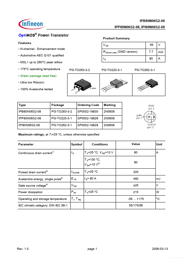
IPB80N06S2-08 IPP80N06S2-08, IPI80N06S2-08
Opti MOS® Power-Transistor
Features
- N-channel
- Enhancement mode
- Automotive AEC Q101 qualified
- MSL1 up to 260°C peak reflow
- 175°C operating temperature
- Green package (lead free)
- Ultra low Rds(on)
- 100% Avalanche tested PG-TO263-3-2
Product Summary V DS R DS(on),max (SMD version) ID 55 7.7 80 V mΩ A
PG-TO220-3-1
PG-TO262-3-1
Type IPB80N06S2-08 IPP80N06S2-08 IPI80N06S2-08
Package PG-TO263-3-2 PG-TO220-3-1 PG-TO262-3-1
Ordering Code SP0002-18830 SP0002-18826 SP0002-18828
Marking 2N0608 2N0608 2N0608
Maximum ratings, at T j=25 °C, unless otherwise specified Parameter Continuous drain current1) Symbol ID Conditions T C=25 °C, V GS=10 V T C=100 °C, V GS=10 V2) Pulsed drain current2) Avalanche energy, single pulse2) Gate source voltage4) Power dissipation Operating and storage temperature IEC climatic category; DIN IEC 68-1 I D,pulse E AS V GS P tot T j, T stg T C=25 °C T C=25 °C I D= 80 A Value 80 80 320 450 ±20 215 -55 ... +175 55/175/56 m J V W °C Unit A
Rev. 1.0 page 1
2006-03-13
Free Datasheet http://.datasheet-pdf./
IPB80N06S2-08 IPP80N06S2-08, IPI80N06S2-08
Parameter Symbol Conditions min. Thermal characteristics2) Thermal resistance, junction
- case Thermal resistance, junction ambient, leaded SMD version, device on PCB R th JC R th JA R th JA minimal footprint 6 cm2 cooling area5) Electrical characteristics, at T j=25 °C, unless otherwise specified Static characteristics Drain-source breakdown voltage Gate threshold voltage Zero gate voltage drain current V (BR)DSS V GS=0 V, I D= 1 m A V GS(th) I DSS V DS=V GS, I D=150 µA V DS=55 V, V GS=0 V, T j=25 °C V DS=55 V, V GS=0 V, T j=125 °C2) Gate-source leakage current Drain-source on-state resistance I GSS RDS(on) V GS=20 V, V DS=0 V V GS=10 V, I D=58 A, V GS=10 V, I D=58 A, SMD version 55 2.1 3.1 0.01 4.0 1 µA V 0.7 62 62 40 K/W Values typ. max. Unit
- 1 1 6.5 6.2
100 100 8.0 7.7 n A mΩ
Rev. 1.0 page 2
2006-03-13
Free Datasheet...