12CN10N
Features
- N-channel, normal level
- Excellent gate charge x R DS(on) product (FOM)
- Very low on-resistance R DS(on)
Product Summary VDS RDS(on),max (TO252) ID
100 V 12.4 m W 67 A
- 175 °C operating temperature
- Pb-free lead plating; Ro HS pliant
- Qualified according to JEDEC1) for target application
- Ideal for high-frequency switching and synchronous rectification
- Halogen-free according to IEC61249-2-21
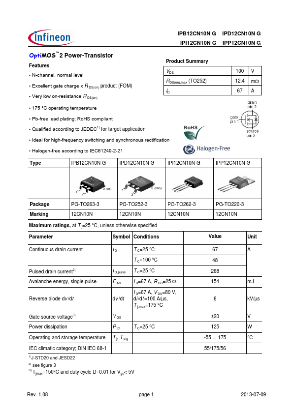
Type
IPB12CN10N G
IPD12CN10N G
IPI12CN10N G
IPP12CN10N G
Package
PG-TO263-3
PG-TO252-3
Marking
Maximum ratings, at T j=25 °C, unless otherwise specified
Parameter
Symbol Conditions
PG-TO262-3 12CN10N
PG-TO220-3 12CN10N
Value
Unit
Continuous drain current
T C=25 °C
T C=100 °C
Pulsed drain current2)
I D,pulse T C=25 °C
Avalanche energy, single pulse
E AS
I D=67 A, R GS=25 W
Reverse diode dv /dt dv /dt
I D=67 A, V DS=80 V, di /dt =100 A/µs, T j,max=175 °C
Gate source voltage3)
V...