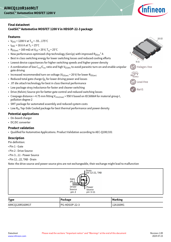
Pin definition:
Pin 1 - Gate
Pin 2 - Drive Source
Pin 311 - Power Source
Pin 1222, TAB - Drain Note: the drive source and power source pins are not exchangeable, their exchange might lead to malfunction
Type AIMCQ120R160M1T
Package PG-HDSOP-22-3
Marking 12A
Key Features
VDSS = 1200 V at Tvj = -55175°C.
IDDC = 18.6 A at TC = 25°C.
RDS(on) = 160 mΩ at VGS = 20 V, Tvj = 25°C.
New performance-optimized chip technology (Gen1p) with improved RDSon.
A.
Best in class switching energy for lower switching losses and reduced cooling efforts.
Lowest device capacitances for higher switching speeds and higher power density.
A combination of low Crss/Ciss ratio and high VGS(th) to avoid parasitic turn-on and.
Full PDF Text Transcription for AIMCQ120R160M1T (Reference)
Note: Below is a high-fidelity text extraction (approx. 800 characters) for
AIMCQ120R160M1T. For precise diagrams, and layout, please refer to the original PDF.
AIMCQ120R160M1T CoolSiC™ Automotive MOSFET 1200 V Final datasheet CoolSiC™ Automotive MOSFET 1200 V in HDSOP-22-3 package Features • VDSS = 1200 V at Tvj = -55...175°C • ...
View more extracted text
in HDSOP-22-3 package Features • VDSS = 1200 V at Tvj = -55...175°C • IDDC = 18.6 A at TC = 25°C • RDS(on) = 160 mΩ at VGS = 20 V, Tvj = 25°C • New performance-optimized chip technology (Gen1p) with improved RDSon* A • Best in class switching energy for lower switching losses and reduced cooling efforts • Lowest device capacitances for higher switching speeds and higher power density • A combination of low Crss/Ciss ratio and high VGS(th) to avoid parasitic turn-on and enable unipolar gate driving • Increased recommended turn-on voltage (VGS(on) = 20 V) for lower RDS(on) • Reduced total gate charge QG for lower driving pow