Infineon Technologies BCV61A
NPN Silicon Double Transistor
| Part No. | BCV61A |
|---|---|
| Datasheet | BCV61A Download |
| Manufacturer |  Infineon Technologies |
| Description | NPN Silicon Double Transistor |
| Buy | Stock & Price |
MAXIMUM RATINGS
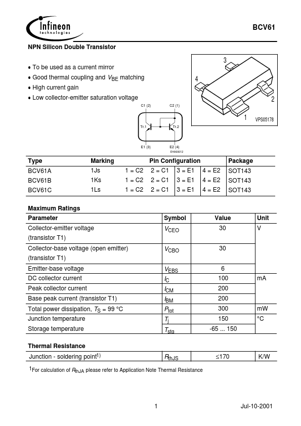
Parameter Marking 1Js 1Ks 1Ls 1 = C2 1 = C2 1 = C2 Pin Configuration 2 = C1 2 = C1 2 = C1 3 = E1 3 = E1 3 = E1 4 = E2 4 = E2 4 = E2 Package SOT143 SOT143 SOT143 Symbol VCEO VCBO VEBS IC ICM IBM Ptot Tj Tstg Value 30 30 6 100 200 200 300 150 -65 ... 150 Unit V Collector-emitter voltage (transistor T1) Collector-base voltage (open emitter) (transistor T1) Emitter-base voltage DC collector current Peak collector current Base peak current (transistor T1) Total power dissipation, TS = 99 °C Junction temperature Storage temperature Thermal Resistance mA mW °C Junction - soldering point1) RthJS 170 K/W 1For calculation of R thJA please refer to Application Note Thermal Resistance 1 Jul-10-2001 BCV61ELECTRICAL CHARACTERISTICS
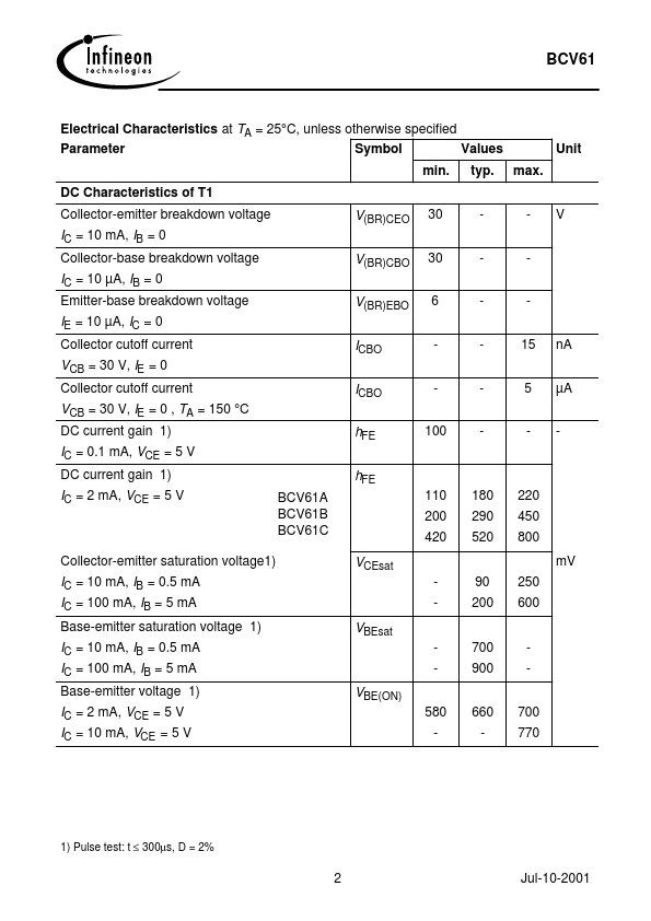
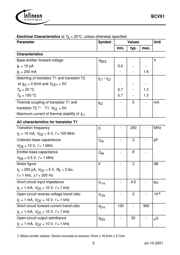
at TA = 25°C, unless otherwise specified Parameter Symbol Values min. DC Characteristics of T1 Collector-emitter breakdown voltage IC = 10 mA, IB = 0 Collector-base breakdown voltage IC = 10 µA, IB = 0 Emitter-base breakdown voltage IE = 10 µA, IC = 0 Col...