Infineon Technologies CFY66-10P
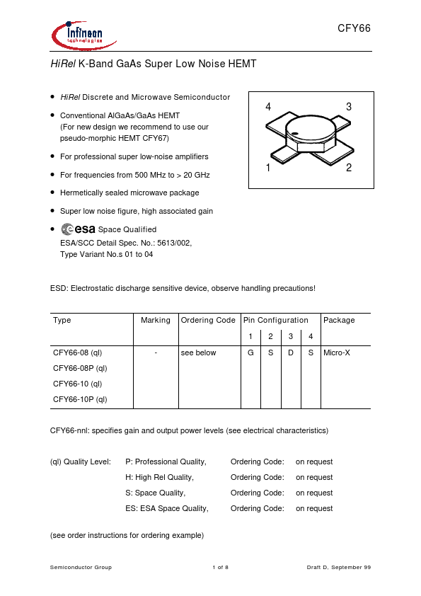
HiRel K-Band GaAs Super Low Noise HEMT
| Part No. | CFY66-10P |
|---|---|
| Datasheet | CFY66-10P Download |
| Manufacturer |  Infineon Technologies |
| Description | HiRel K-Band GaAs Super Low Noise HEMT |
| Buy | Stock & Price |
MAXIMUM RATINGS
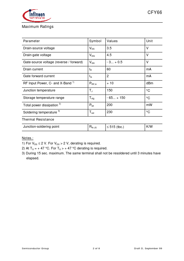
Parameter Drain-source voltage Drain-gate voltage Gate-source voltage (reverse / forward) Drain current Gate forward current RF Input Power, C- and X-Band 1) Junction temperature Storage temperature range Total power dissipation 2) Symbol VDS VDG VGS ID IG PRF,in TJ Tstg Ptot Tsol Values 3.5 4.5 - 3... + 0.5 60 2 + 10 150 - 65... + 150 200 230 Unit V V V mA mA dBm °C °C mW °C Soldering temperature 3) Thermal Resistance Junction-soldering point Notes.: Rth JS ≤ 515 (tbc.) K/W 1) For VDS ≤ 2 V. For VDS > 2 V, derating is required. 2) At TS = + 47 °C. For TS > + 47 °C derating is required. 3) During 15 sec. maximum. The same terminal shall not be resoldered until 3 minutes have elapsed. Semiconductor Group 2 of 8 Draft D, September 99 CFY66ELECTRICAL CHARACTERISTICS
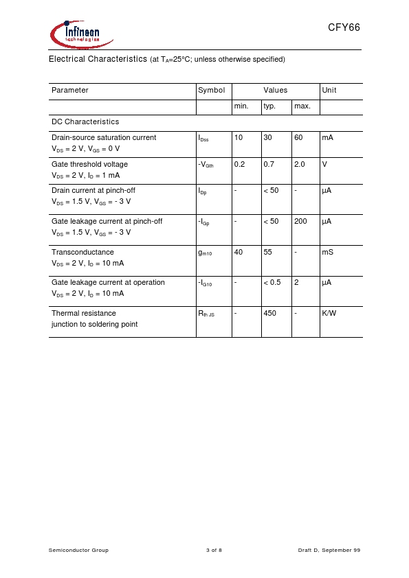
(at TA=25°C; unless otherwise specified) Parameter Symbol min. Values typ. max. Unit DC Characteristics Drain-source saturation current VDS = 2 V, VGS = 0 V Gate threshold voltage VDS = 2 V, ID = 1 mA Drain cu...